Merged control/process element processor for executing VLIW simplex instructions with SISD control/SIMD process mode bit
a control/process element processor and vliw simplex technology, applied in the field of array processing, can solve problems such as overall system inefficiency, and achieve the effect of reducing implementation costs
- Summary
- Abstract
- Description
- Claims
- Application Information
AI Technical Summary
Benefits of technology
Problems solved by technology
Method used
Image
Examples
second embodiment
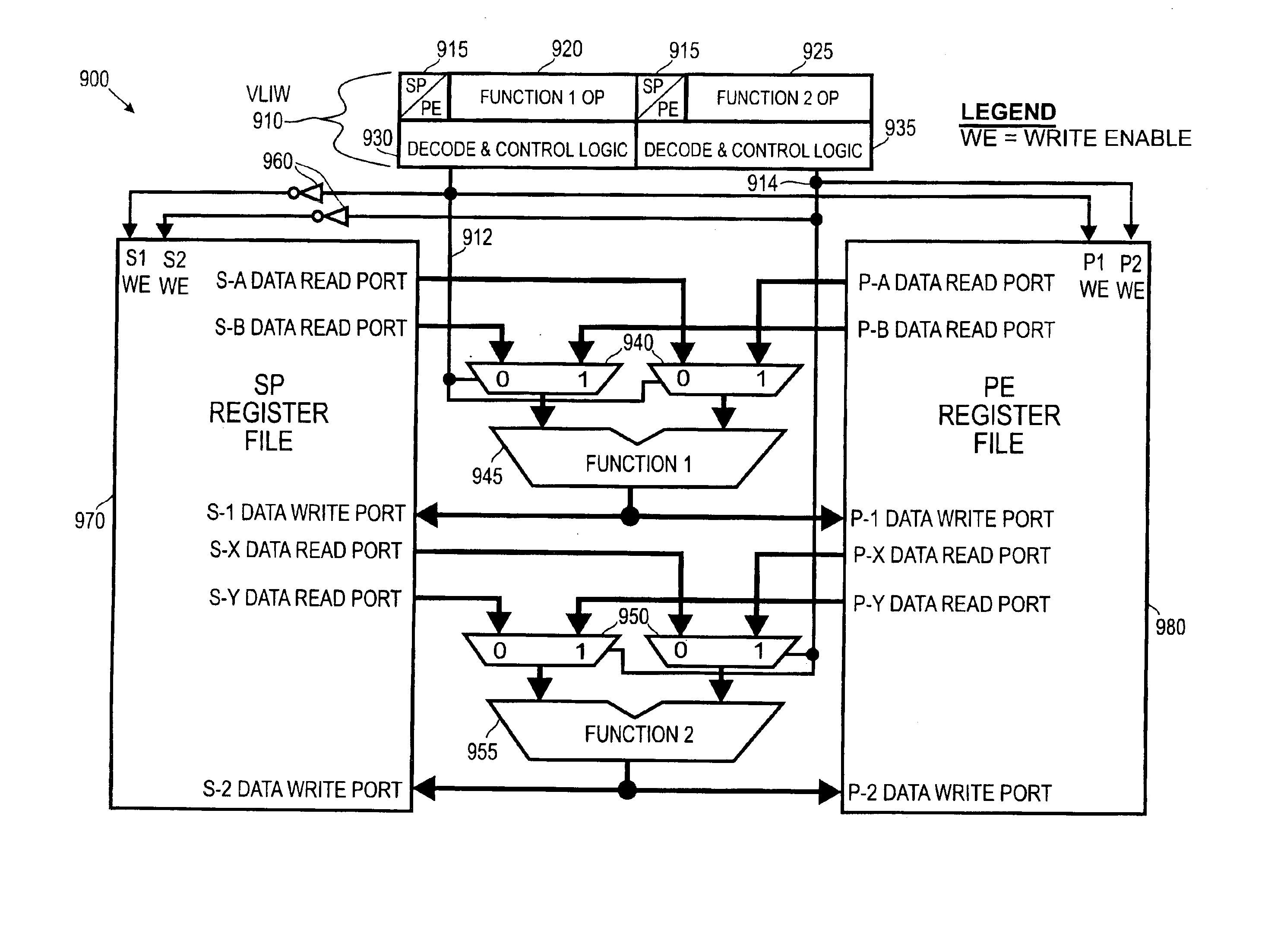
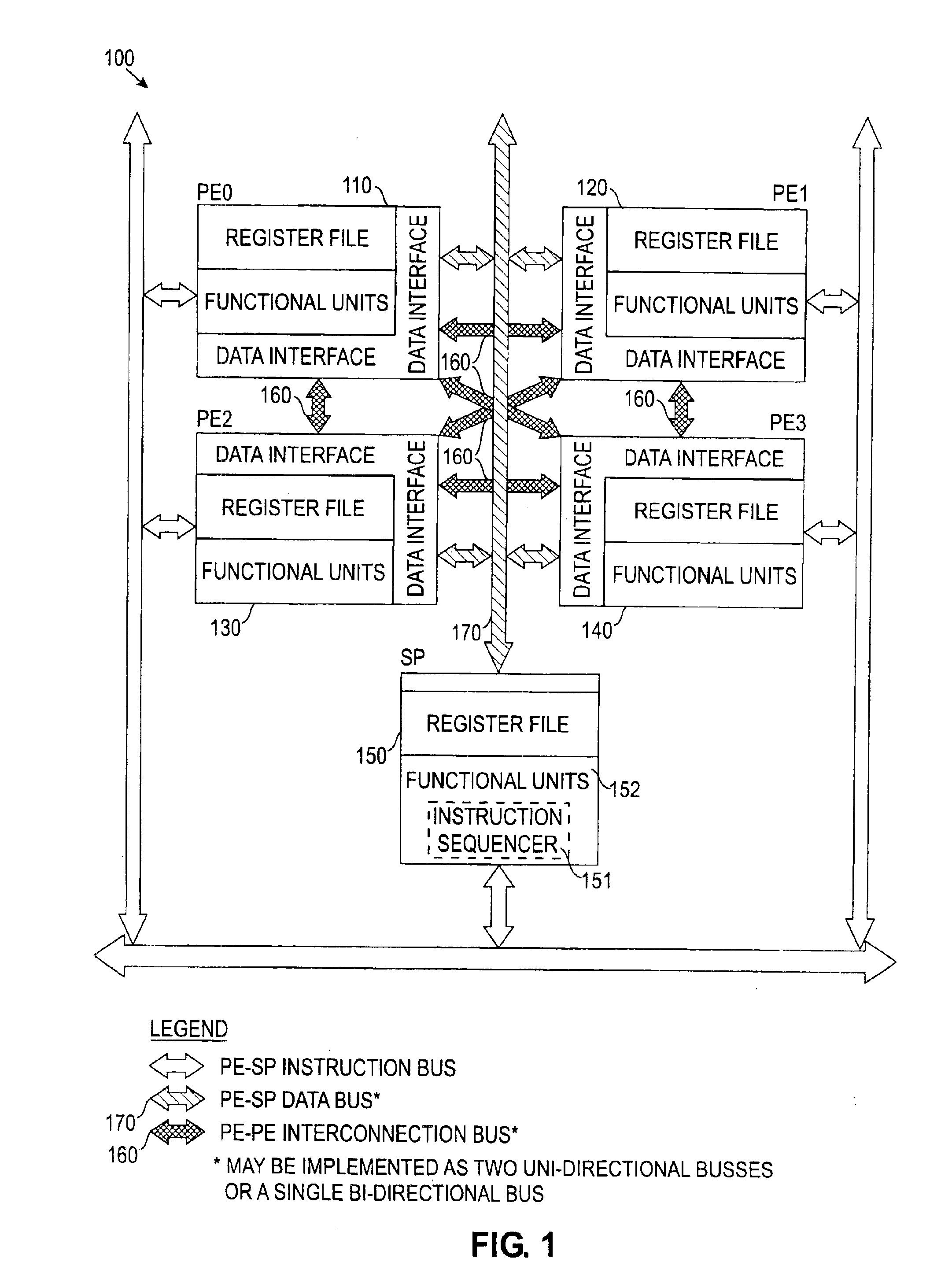
In the present invention shown in FIG. 5, an array 500 includes a DP 510 and PEs 520, 530 and 540. The DP 510 includes a plurality of execution units and a single general-purpose register file. The execution units are “shared” in that they can execute instructions while the processor is in either mode of operation. The register file is divided into two banks, a PE bank and an SP bank, where the two banks are generally “not shared” in the two separate modes of operation. However, both banks are available for data communications in either mode of operation via the array's interconnection network, enabling the exchange of data between PEs or a PE and the SP.
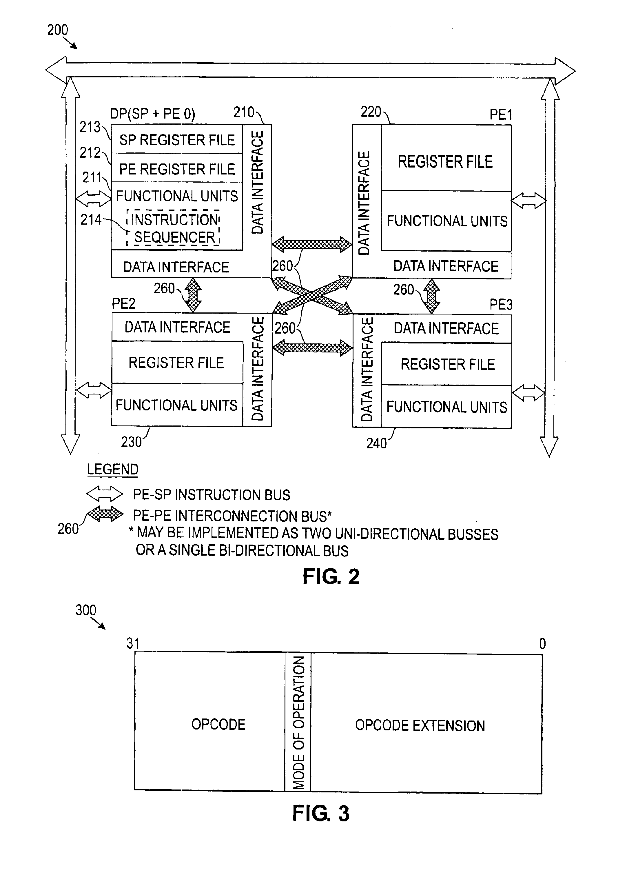
Instruction processing begins with an instruction sequencer 511 which is a part of the functional units block 512 of the DP 510 which operates to fetch instructions. After each instruction is fetched, it is decoded in parallel by the DP and by each PE in the array. In each device, a “mode-of-operation” bit in the instruction word is...
fourth embodiments
In third and fourth embodiments of the present invention, the DP, the array of PE's, and their interconnection network, are implemented in a manner similar to that described in the first and second embodiments of the present invention, respectively. Unlike the implementation of the first two embodiments, however, instead of using a “mode-of-operation” bit in the instruction to determine the register file, or bank, accessed by the DP (or PEs) during an operation, the most-significant bit (MSB) of the source and / or destination register addresses contained in the instruction is used. A suggested instruction format 700 for the operation of these embodiments is shown in FIG. 7.
Instruction processing begins with the instruction sequencer in the DP fetching instructions. As each instruction is fetched, it is decoded in parallel by the DP and by each PE in the array. In each device, the MSB of the source and / or target register addresses in the instruction word is examined to determine the m...
PUM
 Abstract
Description
Claims
Application Information


