Substrate transport container

a technology for transporting containers and substrates, applied in the direction of transportation and packaging, instruments, originals for photomechanical treatment, etc., can solve the problems of loss of resolution, increase in weight of transport containers, and corrosion of wirings

Inactive Publication Date: 2005-04-05
EBARA CORP
View PDF27 Cites 49 Cited by
  • Summary
  • Abstract
  • Description
  • Claims
  • Application Information

AI Technical Summary

Benefits of technology

[0012]This invention is provided in view of the background information described above, and an object of the present invention is to provide a substrate transport container for use in the process of manufacturing integrated circuits of less than 0.13 μm line width, to enable to freely c...

Problems solved by technology

Base gases react with chemical enhancement type photoresist to result in loss of resolution and acidic gases can cause corrosion of wirings.
This is because finer patterning has led to the use of a variety of materials in forming wirings and films, and moisture in the environment can sometimes bind with the above-mentioned materials to cause problems.
Automation of semiconductor manufacturing line is promoted by the fact that it is necessary to segregate humans, who act as a contamination source, and the fact that, as the diameter of the semiconductor wafers increases, the weight of the transport container increases to about 10 kg such that manual handling becomes difficult.
However, when the width of the wires becomes less than 0.13 μm, conventional aluminum wiring causes serious problems of heat generation and signal delay so that, in place of aluminum wiring, there is a trend towards the use of copper wiring, which has lower resistivity than aluminum wiring.
However, the dielectric constant of SiO2, which is at about 4, is high, so that replacement of aluminum wiring with copper wiring only results in about 20% improvement in signal delay.
Prior to such a development, examination of copper wiring and low dielectric materials for insulation has already be...

Method used


Image

  • Substrate transport container
  • Substrate transport container
  • Substrate transport container

Examples


fourth embodiment

[0040]FIG. 27 is a bottom view of the transport container in the present invention;

[0041]FIG. 28A is a diagram to show a check valve of an air inlet port in a closed state, and FIG. 28B shows the valve in an open state;

[0042]FIG. 29A is a diagram to show as check valve of an air outlet port in a closed state, and FIG. 29B shows the valve in and open state;

[0043]FIG. 30 is a diagram to show an example of a wiring circuit forming process for a semiconductor chip using copper wire and a low dielectric insulation film; and

[0044]FIGS. 31A to 31H are diagrams to show various methods for discharging static electricity from the transport container.

DETAILED DESCRIPTION OF THE PREFERRED EMBODIMENTS

[0045]Preferred embodiments will be explained in the following with reference to the drawings attached.

[0046]First, the necessity for a substrate transport container (pod), which is compatible for automation in semiconductor device manufacturing plants, will be explained. To prevent human errors by ...

first embodiment

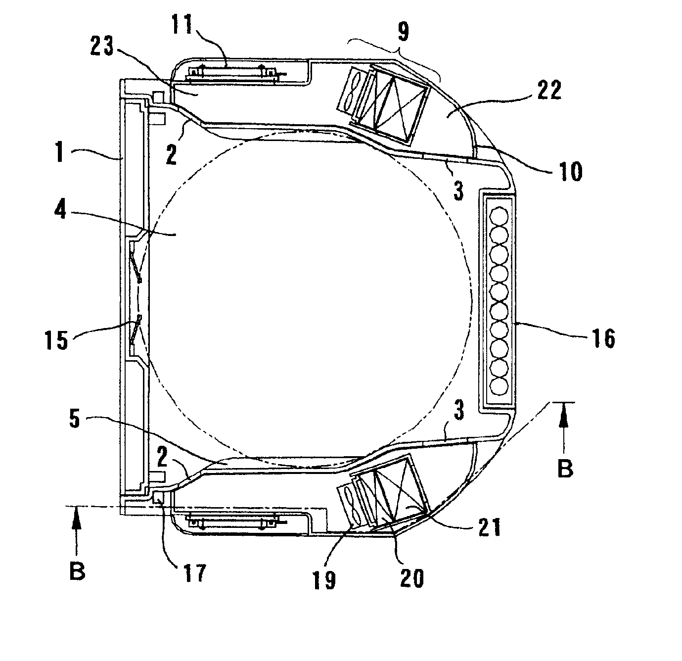
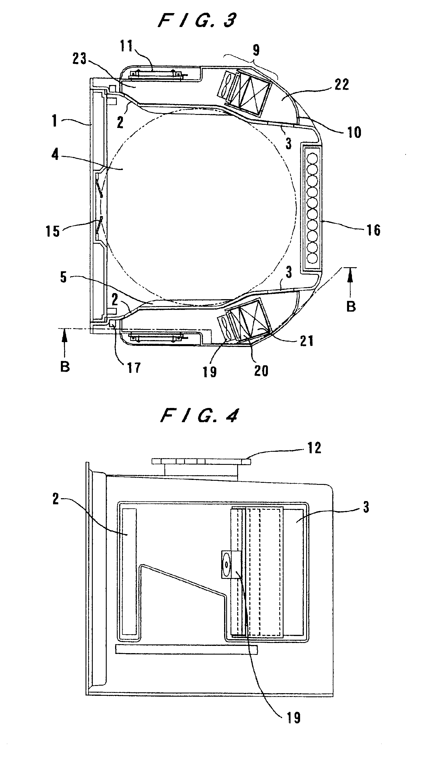
[0049]Next, specific structures of the first embodiment will be explained with reference to FIGS. 1 through 7. The essential components are: a door 1 having a latching mechanism that is operable externally by a locking / unlocking device; a container main body 6 having opening sections 2, 3 for allowing the internal atmosphere of the container main body to communicate with air conditioning means and made as a unit body with a holding device 5 for holding the substrates 4 at a given distance; a bottom surface receptor section 8 having a receptor section 7, for seating the container in a specific location, for engaging with the positioning device of the apparatus; a first air conditioning apparatus 9 disposed on the outer surface of the container main body 6; a cover 10 that covers the first air conditioning apparatus 9 and the opening sections 2, 3 and serves as an isolation wall for the outer environment of the container as well as a circulation path; a second air conditioning apparat...


PUM

PropertyMeasurementUnit
Sizeaaaaaaaaaa
Water absorptionaaaaaaaaaa
Concentrationaaaaaaaaaa

Abstract

A substrate transport container is used, for example, in the process of manufacturing integrated circuits of less than 0.13 μm line width, can hold the level of contaminants in the interior of the container for at least particles, acidic gases, basic gases, organic substances and humidity at controlled low levels, and has the size and structure to be compatible with automated semiconductor manufacturing plants. The container is provided with a door for loading and unloading substrates on a surface of a container main body and is constructed so as to hold the substrates inside the container main body at a given distance of separation. Air conditioning apparatuses for reducing the levels of particulate and gaseous contaminants are disposed roughly symmetrically on the container main body.

Description

[0002]Applicants claim benefit of priority to prior U.S. patent application Ser. No. 60 / 340,503, filed Dec. 19, 2001.BACKGROUND OF THE INVENTION[0003]1. Field of the Invention[0004]The present invention relates to the structures, capabilities and methods of operating a substrate transport container suitable for storing or transporting objects such as semiconductor wafers, photo-masks or hard-disks in a highly clean environment.[0005]2. Description of the Related Art[0006]As pattern sizes of semiconductor devices become finer, it is anticipated that even higher degree of cleanliness would be required in the future. For example, it is anticipated that the target control size of the particulate contaminants that can cause pattern defects and shorting of wiring would become smaller than 0.1 μm. Further, in addition to particulate contaminants, it becomes necessary to reduce gaseous contaminants. By adsorbing onto the semiconductor wafers, various hydrocarbon molecules cause deterioratio...

Claims


Application Information

Patent Timeline
IPC IPC(8): H01L21/673H01L21/67
CPCG03F1/66H01L21/67379H01L21/67393Y10S414/14Y10S414/135
Inventor TANAKA, AKIRASUZUKI, YOKOKISHI, TAKASHI
Owner EBARA CORP
Why Eureka
Try Eureka