Polymer sacrificial light absorbing structure and method

a technology of polymer and light absorbing structure, applied in the direction of chemistry apparatus and processes, crystal growth process, basic electric elements, etc., can solve the problems of increasing complexity of process flow, prohibitively expensive manufacturing environment implementation, and defects known as “shell defects” and “microtrenching” or “cratering”

Inactive Publication Date: 2005-04-05
INTEL CORP
View PDF3 Cites 376 Cited by
  • Summary
  • Abstract
  • Description
  • Claims
  • Application Information

AI Technical Summary

Problems solved by technology

Such process flows are increasingly complex, providing potential sources of defects, and can be prohibitively expensive to implement in a manufacturing environment.
The implementation of BOARC layers in polymer dual damascene patterning, however, has been associated with problems due to inexact matching of etch rate...

Method used


Image

  • Polymer sacrificial light absorbing structure and method
  • Polymer sacrificial light absorbing structure and method
  • Polymer sacrificial light absorbing structure and method

Examples


Embodiment Construction

In the following detailed description of embodiments of the invention, reference is made to the accompanying drawings in which like references indicate similar elements. The illustrative embodiments described herein are disclosed in sufficient detail to enable those skilled in the art to practice the invention. The following detailed description is therefore not to be taken in a limiting sense, and the scope of the invention is defined only by the appended claims.

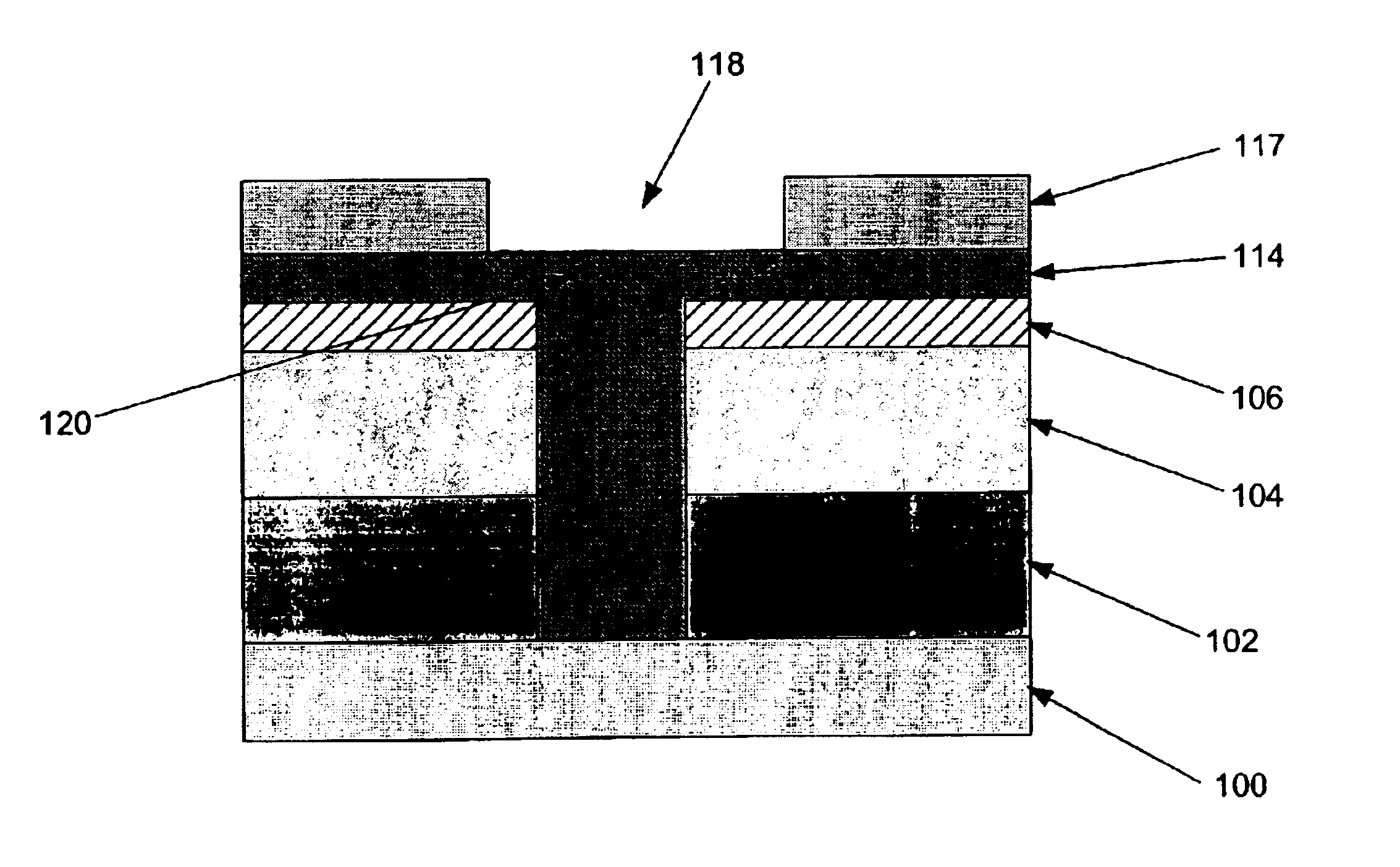
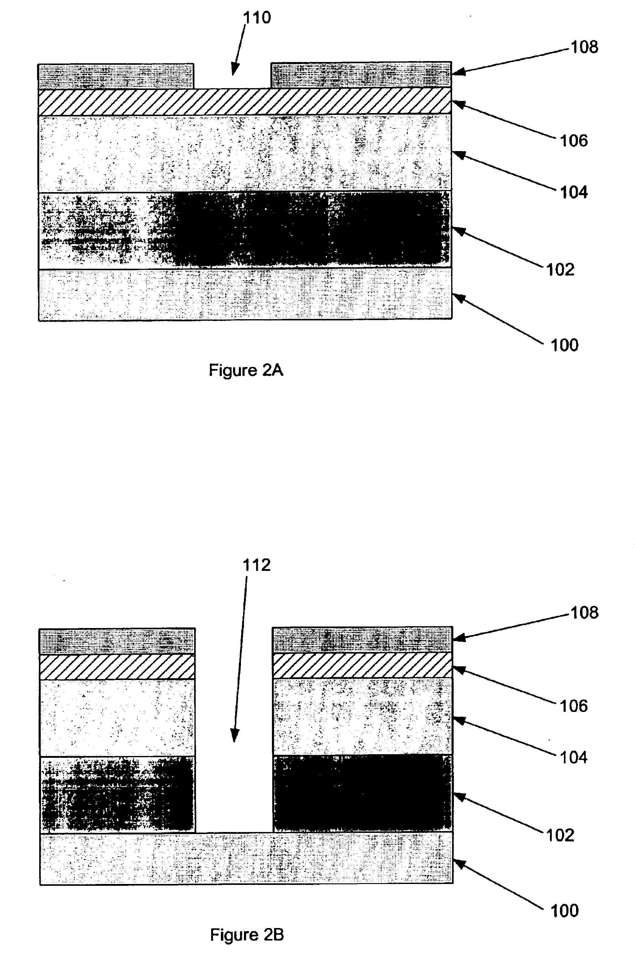
Referring to FIG. 2A, a microelectronic structure, such as a semiconductor structure, is depicted having a substrate layer (100) adjacent a two-part dielectric structure having a first dielectric layer, or “via” dielectric layer (102) for convenience, positioned between the substrate layer (100) and a second, or “line” dielectric layer (104). In another embodiment, the via and line (102, 104) dielectric layers may comprise portions of a single dielectric layer which may be homogeneous or not, as would be apparent to one ski...


PUM


Abstract

Method and structure for optimizing dual damascene patterning with polymeric dielectric materials are disclosed. Certain embodiments of the invention comprise polymeric sacrificial light absorbing materials (“polymer SLAM”) functionalized to have a controllable solubility switch wherein such polymeric materials have substantially the same etch rate as conventionally utilized polymeric dielectric materials, and subsequent to chemical modification of solubility-modifying protecting groups comprising the SLAM materials by thermal treatment or in-situ generation of an acid, such SLAM materials become soluble in weak bases, such as those conventionally utilized to remove materials in lithography treatments.

Description

BACKGROUND OF THE INVENTIONDual damascene interconnects may enable reliable low cost production of integrated microelectronic circuits using sub 0.18 micron process technology. Process flows utilizing sacrificial light absorbing materials (“SLAM”) may be employed to facilitate very small feature size dual damascene interconnects. With such techniques, a first etched region (e.g., a via or trench) may be filled with a sacrificial light absorbing material (“SLAM”), after such region has been formed within a dielectric layer. The SLAM preferably comprises a material having dry etch properties similar to those of the dielectric layer and anti-reflective (or light absorbing) properties that prevent lithographic-related defects during subsequent photoresist processing. After the first etched region is filled with the SLAM, a second etched region (e.g., a trench if the via is already formed or a via if the trench is already formed) may be formed within the dielectric layer. Some of the SLA...

Claims


Application Information

Patent Timeline
IPC IPC(8): C30B1/00H01L29/66H01L27/20H01L29/84H01L21/768
CPCH01L21/76835H01L21/76808
Inventor GOODNER, MICHAEL D.
Owner INTEL CORP
Why Eureka
Try Eureka