
Semiconductor memory device

Inactive Publication Date: 2005-04-05
PANASONIC CORP
View PDF33 Cites 5 Cited by
  • Summary
  • Abstract
  • Description
  • Claims
  • Application Information

AI Technical Summary

Benefits of technology

It is therefore an object of the present invention to reduce the amount of leakage current flowing from the ferroelectric layer of an FeFET memory toward the gate electrode thereof and thereby improve the retention characteristics of the memory greatly.
In the first inventive memory device, the first insulating layer that is insulated against a leakage current more fully than the ferroelectric layer exists between the ferroelectric layer and the gate electrode. Thus, the leakage current flowing from the ferroelectric layer toward the gate electrode can be reduced considerably, thus improving the retention characteristics of the FeFET memory greatly.
Then, the leakage current flowing from the ferroelectric layer toward the semiconductor substrate can also be reduced, thus further improving the retention characteristics of the FeFET memory.
Then, the voltage applied to the ferroelectric layer can be kept higher compared to a situation where a gate voltage of the same level is applied with another insulator with good insulating properties (e.g., silicon dioxide) used for the first insulating layer in the same device structure. This is because an oxide containing strontium and tantalum has good insulating properties as well as a high dielectric constant.
In the second inventive memory device, the ferroelectric layer is covered with an insulating layer, which is insulated against a leakage current more fully than the ferroelectric layer. Thus, the amount of leakage current flowing from the ferroelectric layer toward the gate electrode or from the ferroelectric layer in all directions can be reduced considerably, thus improving the retention characteristics of the FeFET memory greatly.
Then, the voltage applied to the ferroelectric layer can be kept higher compared to a situation where a gate voltage of the same level is applied with another insulator with good insulating properties (e.g., silicon dioxide) used for the insulating layer in the same device structure. This is because an oxide containing strontium and tantalum has good insulating properties as well as a high dielectric constant.

Problems solved by technology

The difficulty in downsizing a memory is a common problem for both FeRAMs and DRAMs alike, and should constitute a serious obstacle to further increasing the density or capacity of a memory in the near future.
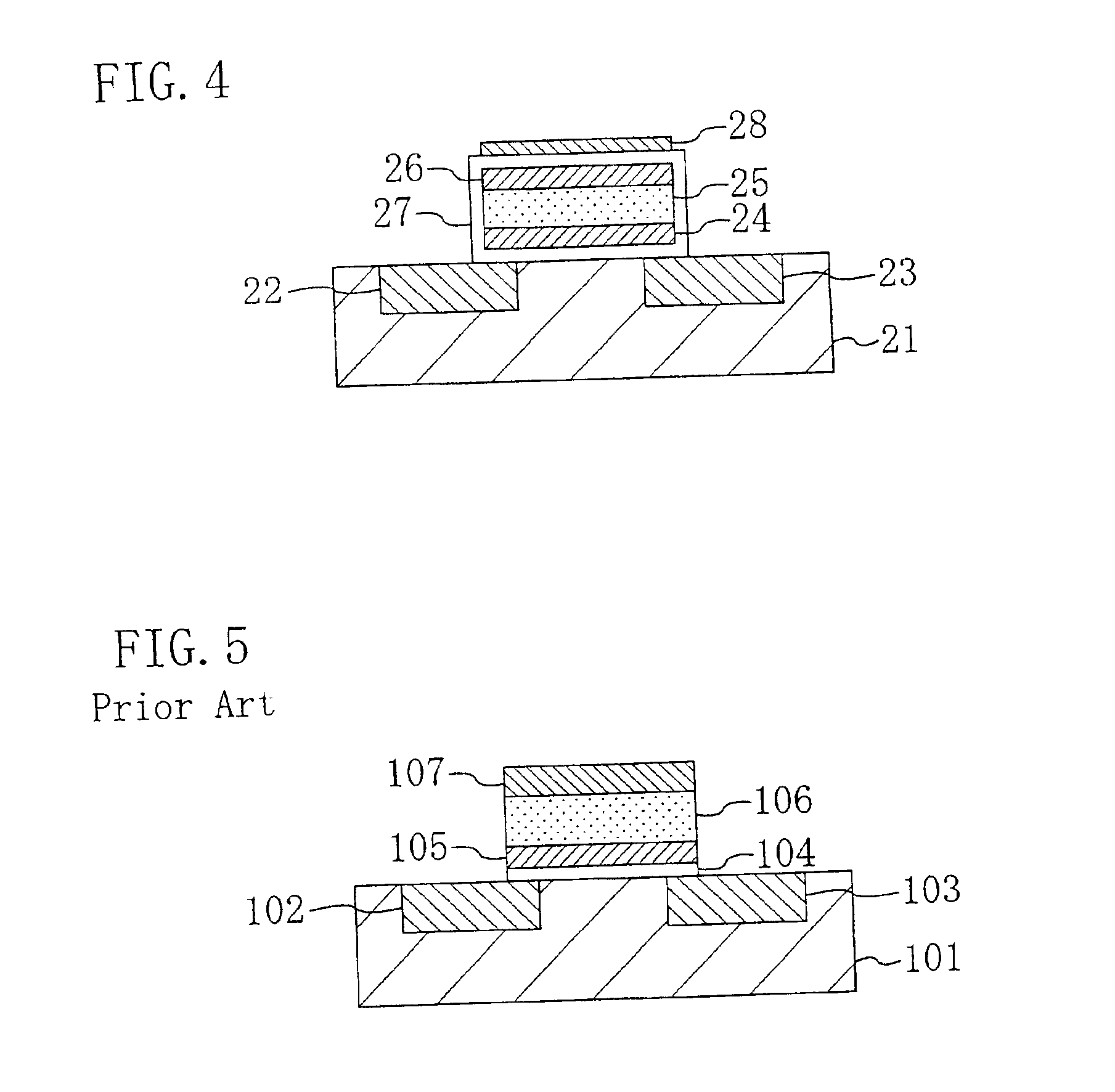
However, it is difficult to realize a good leakage current characteristic for the ferroelectric layer 106 in the present circumstances.

Method used


Image

  • Semiconductor memory device
  • Semiconductor memory device
  • Semiconductor memory device

Examples


embodiment 1

Hereinafter, a semiconductor memory device according to a first embodiment of the present invention will be described with reference to the accompanying drawings.

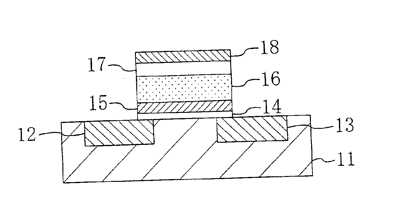
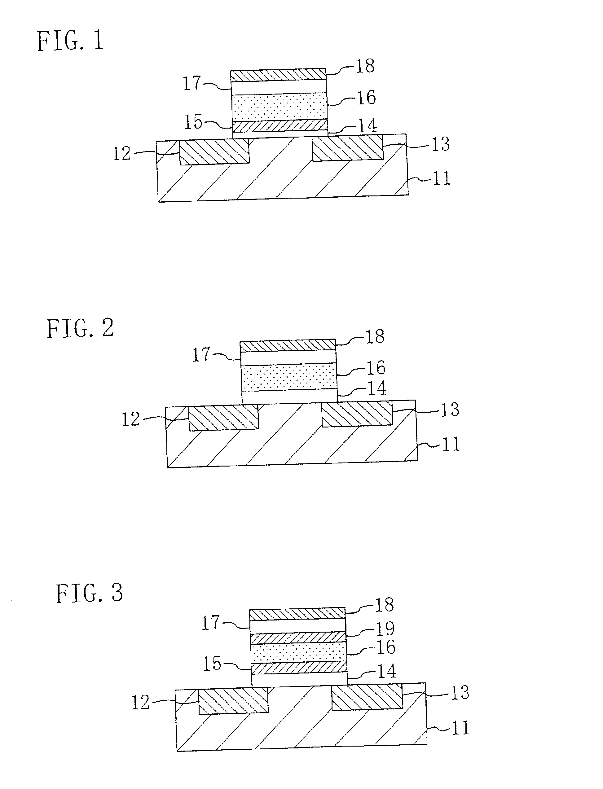
FIG. 1 is a cross-sectional view showing a cell structure for a semiconductor memory device according to the first embodiment, specifically, a cell structure for an FeFET memory.

As shown in FIG. 1, lower insulating layer 14, floating gate 15, ferroelectric layer 16, upper insulating layer 17 and gate electrode 18 are stacked in this order on a semiconductor substrate 11 in which source and drain regions 12 and 13 are defined. In this structure, the lower insulating layer 14 and the upper insulating layer 17 are insulated against leakage current more fully than the ferroelectric layer 16.

In the memory cell of the embodiment shown in FIG. 1, a voltage is applied between the gate electrode 18 and the semiconductor substrate 11 so that one of the gate electrode 18 and the semiconductor substrate 11 is at a positive or negative ...

modified example 1 of embodiment 1

Hereinafter, a semiconductor memory device according to a first modified example of the first embodiment will be described with reference to the accompanying drawings.

FIG. 2 is a cross-sectional view showing a cell structure for a semiconductor memory device according to the first modified example, specifically, a cell structure for an FeFET memory. In FIG. 2, each member also shown in FIG. 1 is identified by the same reference numeral and the description thereof will be omitted herein.

The first embodiment relates to an FeFET memory (see FIG. 1) including the floating gate 15, while the first modified example of the first embodiment relates to an FeFET memory including no floating gate 15. That is to say, the only difference between the first embodiment and the first modified example is that the floating gate 15 is not included in the first modified example shown in FIG. 2.

In this first modified example of the first embodiment, the voltage applied to the ferroelectric layer 16 is al...

modified example 2 of embodiment 1

Hereinafter, a semiconductor memory device according to a second modified example of the first embodiment will be described with reference to the accompanying drawings.

FIG. 3 is a cross-sectional view showing a cell structure for a semiconductor memory device according to the second modified example, specifically, a cell structure for an FeFET memory. In FIG. 3, each member also shown in FIG. 1 is identified by the same reference numeral and the description thereof will be omitted herein.

The first embodiment relates to an FeFET memory (see FIG. 1) including one floating gate 15, while the second modified example of the first embodiment relates to an FeFET memory including two floating gates. That is to say, the only difference between the first embodiment and the second modified example is that an upper floating gate 19 is formed between the ferroelectric layer 16 and the upper insulating layer 17, in addition to the floating gate 15, in the second modified example as shown in FIG. ...


PUM


Abstract

A semiconductor memory device includes a field-effect transistor with a gate electrode that has been formed over a semiconductor substrate with a ferroelectric layer interposed between the electrode and the substrate. The device includes a first insulating layer, which is insulated against a leakage current more fully than the ferroelectric layer, between the ferroelectric layer and the gate electrode.

Description

BACKGROUND OF THE INVENTIONThe present invention relates to a semiconductor memory device including a field-effect transistor with a gate electrode that has been formed over a semiconductor substrate with a ferroelectric layer interposed between the electrode and the substrate.Recently, ferroelectric random-access memories (which will be herein referred to as “FeRAMs”) for use in IC cards or portable electronic units have been developed by semiconductor manufacturers. FeRAMs are nonvolatile memories, i.e., some contents stored thereon are not lost even when power is removed, and yet can operate almost as fast as DRAMs.Most of the FeRAMs currently under development have either a two-transistor two-capacitor (2T2C) memory cell structure or a one-transistor one-capacitor (1T1C) memory cell structure. Therefore, in order to downsize FeRAMs, advanced patterning technology, including a technique of realizing a stereoscopic capacitor structure, is required. The difficulty in downsizing a m...

Claims


Application Information

Patent Timeline
IPC IPC(8): H01L29/66H01L29/51H01L29/78H01L29/40H01L29/788B65G1/137G11C11/22H01L21/8246H01L21/8247H01L27/105H01L29/792
CPCH01L29/516H01L29/78391H01L29/7881G11C11/22
Inventor UCHIYAMA, KIYOSHISHIMADA, YASUHIROARITA, KOJIOTSUKI, TATSUO
Owner PANASONIC CORP
Learn More