Voltage tunable laminated dielectric materials for a coplanor waveguide

a technology of laminated dielectric materials and coplanar waveguides, which is applied in the direction of waveguides, waveguide type devices, high frequency circuit adaptations, etc., can solve the problems of low antenna efficiencies, high dielectric constants are not suitable, and complex fabrication of such devices

Inactive Publication Date: 2005-04-05
NXP USA INC
View PDF3 Cites 36 Cited by
  • Summary
  • Abstract
  • Description
  • Claims
  • Application Information

AI Technical Summary

Benefits of technology

This invention provides a tunable dielectric structure including a first layer off dielectric material, and a second layer of dielectric material positioned adjacent to the first layer of dielectric material, with the second layer of dielectric material having a dielectric constant that is less than the dielectric constant of the first layer of dielectric material. The structure further includes electrodes for applying a controllable voltage across the first dielectric material, thereby controlling a dielectric constant of the first dielectric material, wherein at least one of the electrodes is positioned between the first and second layers of dielectric material.

Problems solved by technology

This makes fabrication of such devices complex.
The high dielectric constant is not suitable for some microwave applications such as patch antennas, which lower the antennas' efficiencies.
High dielectric constant materials also cause low characteristic impedance (<10 Ω) in microstrip, coplanar, and other planar structure transmission lines, which strongly limits the application of high dielectric constant materials.

Method used


Image

  • Voltage tunable laminated dielectric materials for a coplanor waveguide
  • Voltage tunable laminated dielectric materials for a coplanor waveguide
  • Voltage tunable laminated dielectric materials for a coplanor waveguide

Examples


Embodiment Construction

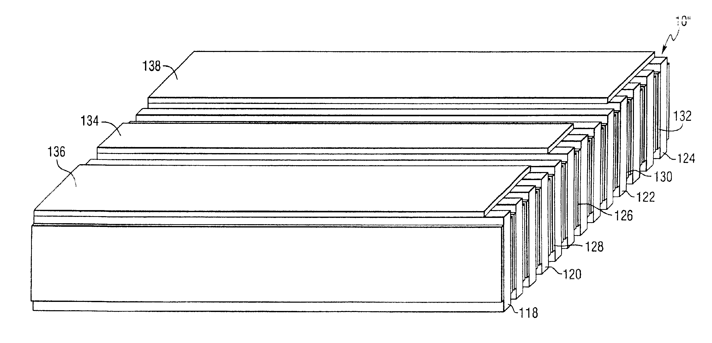
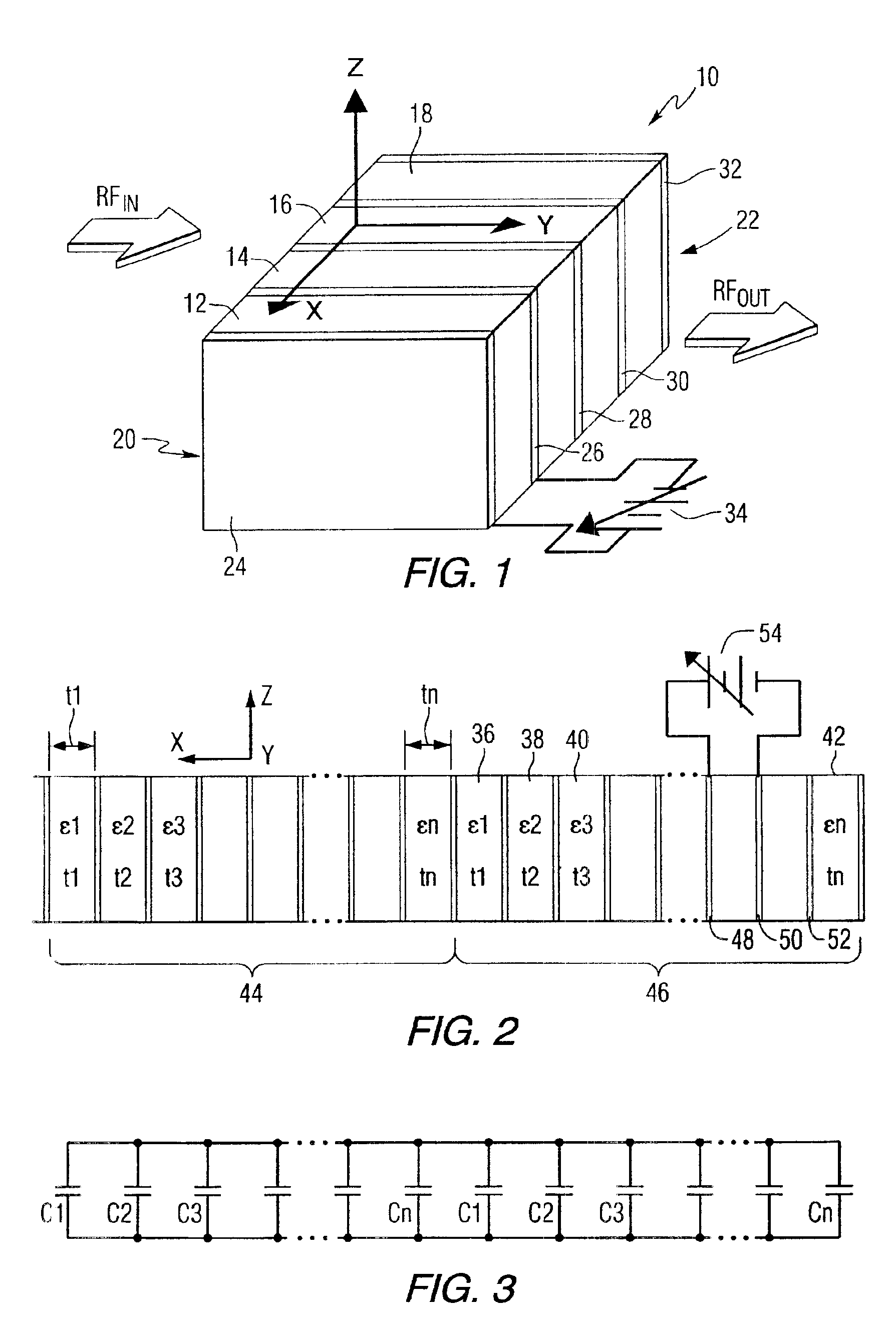
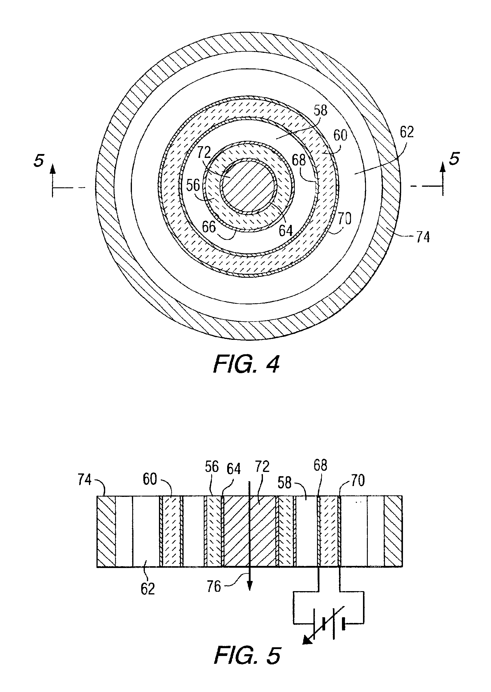
Referring to the drawings, FIG. 1 is an isometric view of an electronic device having a dielectric structure of laminated materials constructed in accordance with a preferred embodiment of the invention. The tunable dielectric device 10 comprises a multilayered structure of dielectric materials 12, 14, 16, 18 including two or more materials having different dielectric constants, and being laminated together to tailor the overall dielectric constant and tunability. One or more materials (e.g. 12 and 16) in the laminated structure are tunable dielectric materials usually with a high dielectric constant, low losses, and high tunability. For the purposes of this description, a high dielectric constant is greater than about 100, low loss materials have loss tangents (tan δ) of less than about 0.01, and tunability of greater than about 15% at 2 V / μm. The high dielectric constant, low loss and high tunability materials may be Ba1-xSrxTiO3 (BSTO), where x can vary between zero and one, and ...


PUM

PropertyMeasurementUnit
dielectric constantaaaaaaaaaa

Abstract

A tunable dielectric structure includes a first layer of dielectric material, a second layer of dielectric material positioned adjacent to the first layer of dielectric material, with the second layer of dielectric material having a dielectric constant that is less than the dielectric constant of the first layer of dielectric material, and electrodes for applying a controllable voltage across the first dielectric material, thereby controlling a dielectric constant of the first dielectric material, wherein at least one of the electrodes is positioned between the first and second layers of dielectric material. The dielectric materials can be formed in various shapes and assembled in various orientations with respect to each other. The tunable dielectric structure is used in various devices including coaxial cables, cavity antennas, microstrip lines, coplanar lines, and waveguides.

Description

BACKGROUND OF INVENTIONThe present invention relates generally to electronic materials for microwave applications, and more particularly to such materials including ferroelectric materials having a tunable dielectric constant.Tunable ferroelectric materials are the materials whose permittivity (more commonly called dielectric constant) can be varied by varying the strength of an electric field to which the materials are subjected or immersed. Even though these materials work in their paraelectric phase above Curie temperature, they are conveniently called “ferroelectric” because they exhibit spontaneous polarization at temperatures below the Curie temperature. Typical tunable ferroelectric materials are barium-strontium titanate (BST) or BST composites. Examples of such materials can be found in U.S. Pat. Nos. 5,312,790, 5,427,988, 5,486,491 and 5,643,429. These materials, especially BSTO-MgO composites, show low dielectric loss and high tunability. Tunability is defined as the frac...

Claims


Application Information

Patent Timeline
Patent Type & Authority Patents(United States)
IPC IPC(8): H01P3/12H01P3/08H01P7/00H01P3/00H01P3/02H01Q3/44H01P3/06H01P7/06H01Q3/00H01P1/18H05K1/16H05K1/02B32B7/02H01P3/16
CPCH01P1/181H01P3/003H01P3/06H01P3/081H01P3/088H01P3/122H01Q3/44H05K1/162H01P7/06H05K2203/171H05K1/024H05K2201/0187H05K2201/037H05K2203/105H01P1/203
Inventor SENGUPTA, LOUISESTOWELL, STEVEN C.ZHU, YONGFEISENGUPTA, SOMNATHCHIU, LUNA H.ZHANG, XUBAI
Owner NXP USA INC
Why Eureka
Try Eureka