Method of making a solid state inductor

Inactive Publication Date: 2005-04-05
SHARP LAB OF AMERICA
View PDF1 Cites 17 Cited by
  • Summary
  • Abstract
  • Description
  • Claims
  • Application Information

AI Technical Summary

Benefits of technology

The present invention describes a solid-state inductor, which has a relatively high inductance value, requires a very small area, and is suitable to be int

Problems solved by technology

Besides using a great amount of valuable IC area, the large-sized inductors generate parasitic reactances and unintended mutual inductances with components that are adjacent, overlying, or underlying the

Method used


Image

  • Method of making a solid state inductor
  • Method of making a solid state inductor
  • Method of making a solid state inductor

Examples


Embodiment Construction

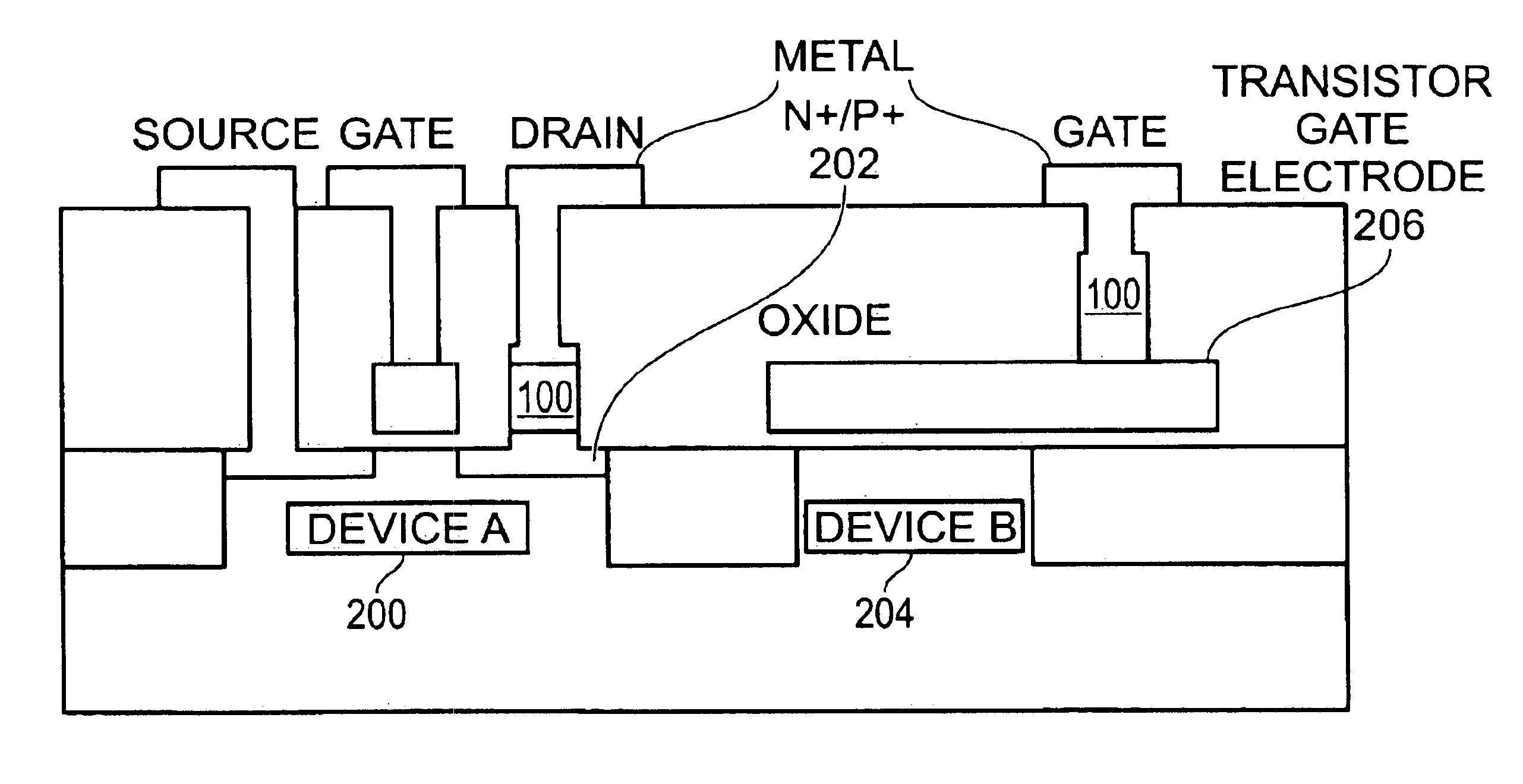
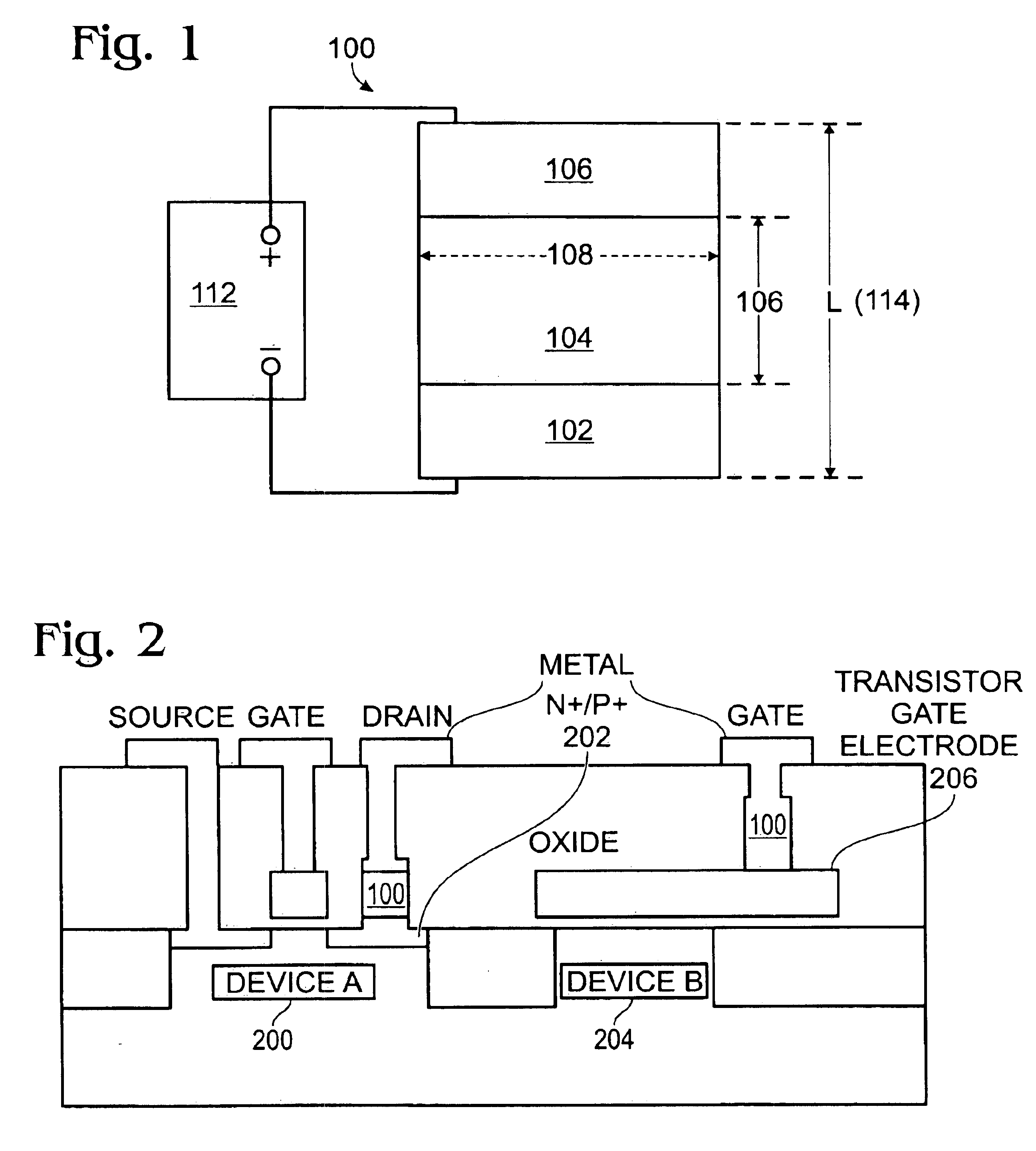
FIG. 1 is a diagram of the present invention solid-state inductor. The inductor 100 comprises a bottom electrode 102 and an electric field-treated colossal magnetoresistance (CMR) thin film 104 overlying the bottom electrode 102. A top electrode 106 overlies the CMR thin film 104.

The CMR thin film 104 is made from a material such as Pr0.3Ca0.7MnO3 (PCMO), La0.7Ca0.3MnO3 (LCMO), Y1-xCaxMnO3 (YCMO), or high-temperature super conductor (HTSC) materials. However, other equivalent materials might also be practical, depending upon requirements. The CMR thin film 104 has a thickness 108 of approximately 2000 Å.

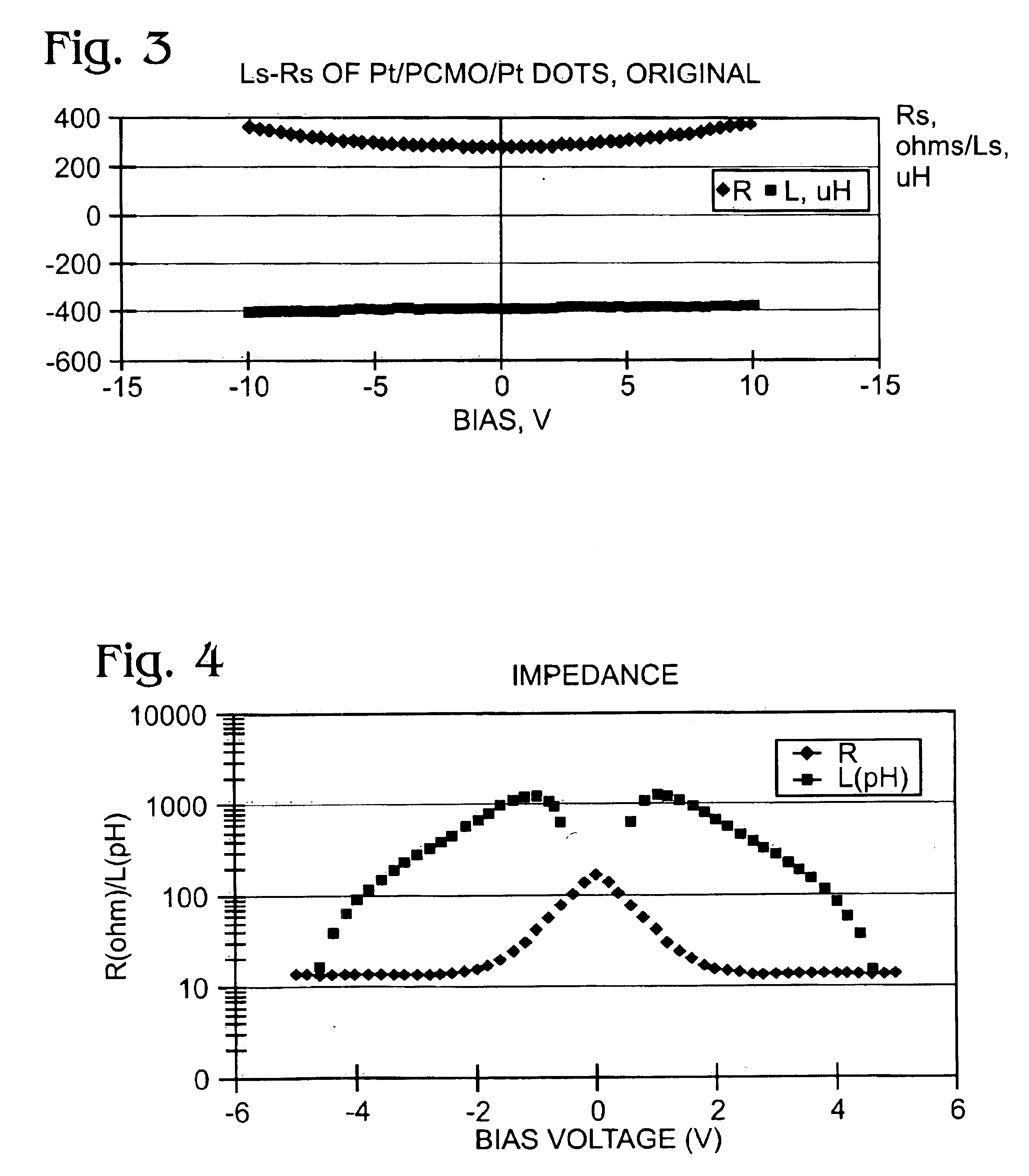
As explained in more detail below, the CMR thin film 104 has been previously exposed to an electric field in the range of 0.4 to 1 megavolts per centimeter (MV / cm), with a pulse width in the range of 100 nanoseconds (ns) to 1 millisecond (ms). This is just an exemplary treatment. Other means of treatment are practical and depend upon the CMR material, intervening materials, and the d...


PUM

PropertyMeasurementUnit
Timeaaaaaaaaaa
Timeaaaaaaaaaa
Electrical inductanceaaaaaaaaaa

Abstract

A solid-state inductor and a method for forming a solid-state inductor are provided. The method comprises: forming a bottom electrode; forming a colossal magnetoresistance (CMR) thin film overlying the bottom electrode; forming a top electrode overlying the CMR thin film; applying an electrical field treatment to the CMR thin film in the range of 0.4 to 1 megavolts per centimeter (MV/cm) with a pulse width in the range of 100 nanoseconds (ns) to 1 millisecond (ms); in response to the electrical field treatment, converting the CMR thin film into a CMR thin film inductor; applying a bias voltage between the top and bottom electrodes; and, in response to the applied bias voltage, creating an inductance between the top and bottom electrodes. When the applied bias voltage is varied, the inductance varies in response.

Description

BACKGROUND OF THE INVENTION1. Field of the InventionThis invention generally relates to semiconductor fabrication and, more particularly, to a solid-state inductor for analog integrated circuit (IC) fabrication and a method for processing the same.2. Description of the Related ArtConventionally, an IC integrated inductor is formed from a metal line, designed in spiral form, overlying a thick layer of insulator on silicon substrate. The inductance value of an inductor so formed is very low, so that the formation of a practical inductor requires a large silicon area. Besides using a great amount of valuable IC area, the large-sized inductors generate parasitic reactances and unintended mutual inductances with components that are adjacent, overlying, or underlying the inductor.Further, a conventional inductor is a passive component, meaning that once it is formed in the IC, the inductance value cannot be changed. Thus, the inductor cannot be used for frequency tuning. Frequency tuning ...

Claims


Application Information

Patent Timeline
IPC IPC(8): H01L27/08H01F10/193H01F21/00H01F41/24H01L21/02
CPCG11C13/0007H01L27/08H01L28/10G11C2213/31H01F10/193Y10T29/4902H01F41/24H01F21/00H01F27/245
Inventor PAN, WEIHSU, SHENG TENGZHUANG, WEI-WEI
Owner SHARP LAB OF AMERICA
Why Eureka
Try Eureka