Electronic antenna module optimised for a chip card with a dual communication interface

Active Publication Date: 2020-12-17
SMART PACKAGING SOLUTIONS SPS
View PDF0 Cites 0 Cited by
  • Summary
  • Abstract
  • Description
  • Claims
  • Application Information

AI Technical Summary

Benefits of technology

[0017]A particular aim of the invention is to provide an electronic module for a smart card with a dual contact and contactless communication interface, having higher inductance values than in the prior art, to compensate for the reduction in the size of the modules, in particular the six-contact modules of dimensions 8.3×11 mm2 used in banking applications.
[0018]Another particular aim of the invention is to propose an electronic module with a dual contact and contactless communication interface which makes it possible to present several inductance values of the ant

Problems solved by technology

When the smart card includes an antenna implemented in the card body, it is sometimes directly connected to the contactless interface of the microelectronic module, and this mechanical connection between the antenna and the module then induces losses of reliability or manufacturing efficiency.
In fact, the mechanical and thermal stresses imposed on the card during its use can cause the connection between the module and the antenna to break, or cause significant increases of the electrical resistance of this connection, resulting in a loss of performance of the card during use.
But new problems have emerged.
Thus, the modules with double communication Interface having metal contacts on their upper face and a microelectronic chip as well as antenna tracks of the module located on their lower face, the electrical connection of the terminals of the chip with the contacts and the antenna

Method used


Image

  • Electronic antenna module optimised for a chip card with a dual communication interface
  • Electronic antenna module optimised for a chip card with a dual communication interface
  • Electronic antenna module optimised for a chip card with a dual communication interface

Examples


Embodiment Construction

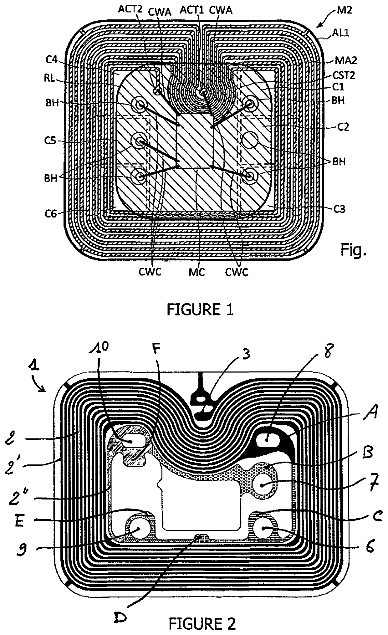
[0040]FIG. 1 corresponds to FIG. 7 of document FR 12 01866 A1 describing an electronic module for a smart card conforming to the state of the art. The module M2 includes a set of 8 turns MA2, extending between the distal end, which is the end of the external turn, denoted ACT1, and the proximal end, which is the end of the internal turn, denoted ACT2. The turns have an offset in the direction of the microelectronic chip denoted MC, and passing through the triangle formed by the distal end ACT and the connection wells of the metal contacts referenced C1 and C4. The distal ACT1 and proximal ACT2 ends of the antenna are clearly inside the encapsulation zone denoted RL, which corresponds to a drop of resin protecting the chip and its connection pads. The access wells BH to the contacts are aligned in two vertical rows on either side of the chip, therefore the triangle formed by ACT and the two upper wells BH which are closest to ACT is of reduced size, which reduces the width available ...


PUM


Abstract

An electronic module for a smart card has on a first face a terminal block of electrical contacts for contact with corresponding contacts of a card reader, and on a second face an antenna and a microelectronic chip within an encapsulation zone and provided with contact and contactless communication interfaces. The antenna has a plurality of turns at the periphery of the module and a proximal connection pad and a distal connection pad inside the encapsulation zone for connection to corresponding terminals of the contactless communication interface. The distal connection pad is located a short distance d from the edge of the encapsulation zone, and the internal edges of connection wells of the two contacts closest to the distal connection pad are spaced outward from the module relative to the internal edges of the connection wells of the other contacts.

Description

[0001]The invention relates to an electronic module with a dual contact and contactless communication interface, and a smart card incorporating such a module.STATE OF THE ART[0002]In the state of the art there are already mixed contact and contactless smart cards. Most have a microelectronic module having on the one hand contacts standardized according to ISO 7816-2 and corresponding to the contacts of a smart card reader, and having on the other hand a radio frequency communication interface provided with at least an antenna and able to communicate with the antenna of a contactless reader.[0003]When the smart card includes an antenna implemented in the card body, it is sometimes directly connected to the contactless interface of the microelectronic module, and this mechanical connection between the antenna and the module then induces losses of reliability or manufacturing efficiency. In fact, the mechanical and thermal stresses imposed on the card during its use can cause the conne...

Claims


Application Information

Patent Timeline
IPC IPC(8): G06K19/07H01Q7/00H05K1/02
CPCH05K1/0243H01Q7/00G06K19/07H05K2201/10098G06K19/07749G06K19/07754G06K19/07769
Inventor CALVAS, BERNARDGERIN, GUILLAUMEFABRIZIO, KEVIN
Owner SMART PACKAGING SOLUTIONS SPS
Why Eureka
Try Eureka