On-chip inductors

Inactive Publication Date: 2007-02-06
NEWPORT FAB
View PDF11 Cites 5 Cited by
  • Summary
  • Abstract
  • Description
  • Claims
  • Application Information

AI Technical Summary

Benefits of technology

[0020]The present invention is method for fabrication of on-chip inductors and related structure. The invention overcomes a serious need in the art for

Problems solved by technology

Thus, the inductor's size limits the use of on-chip inductors for RF and mixed signal circuits.
However, this would make the on-chip inductor even larger and would require more chip space.
Therefore, there is little available space on the chip for even larger inductors.
Thus, it is seen that there are problems associated with both of the above described methods for increasing the inductance of a square spiral inductor.
However, the reduction in the size of on-chip inductors that has been achieved by these variations in the layout of the inductor has been outpaced by the contin

Method used


Image

  • On-chip inductors
  • On-chip inductors
  • On-chip inductors

Examples


Embodiment Construction

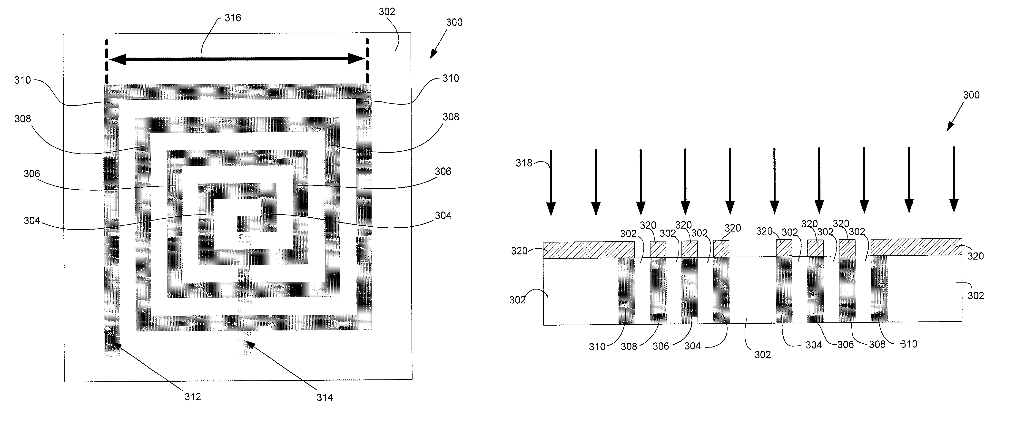
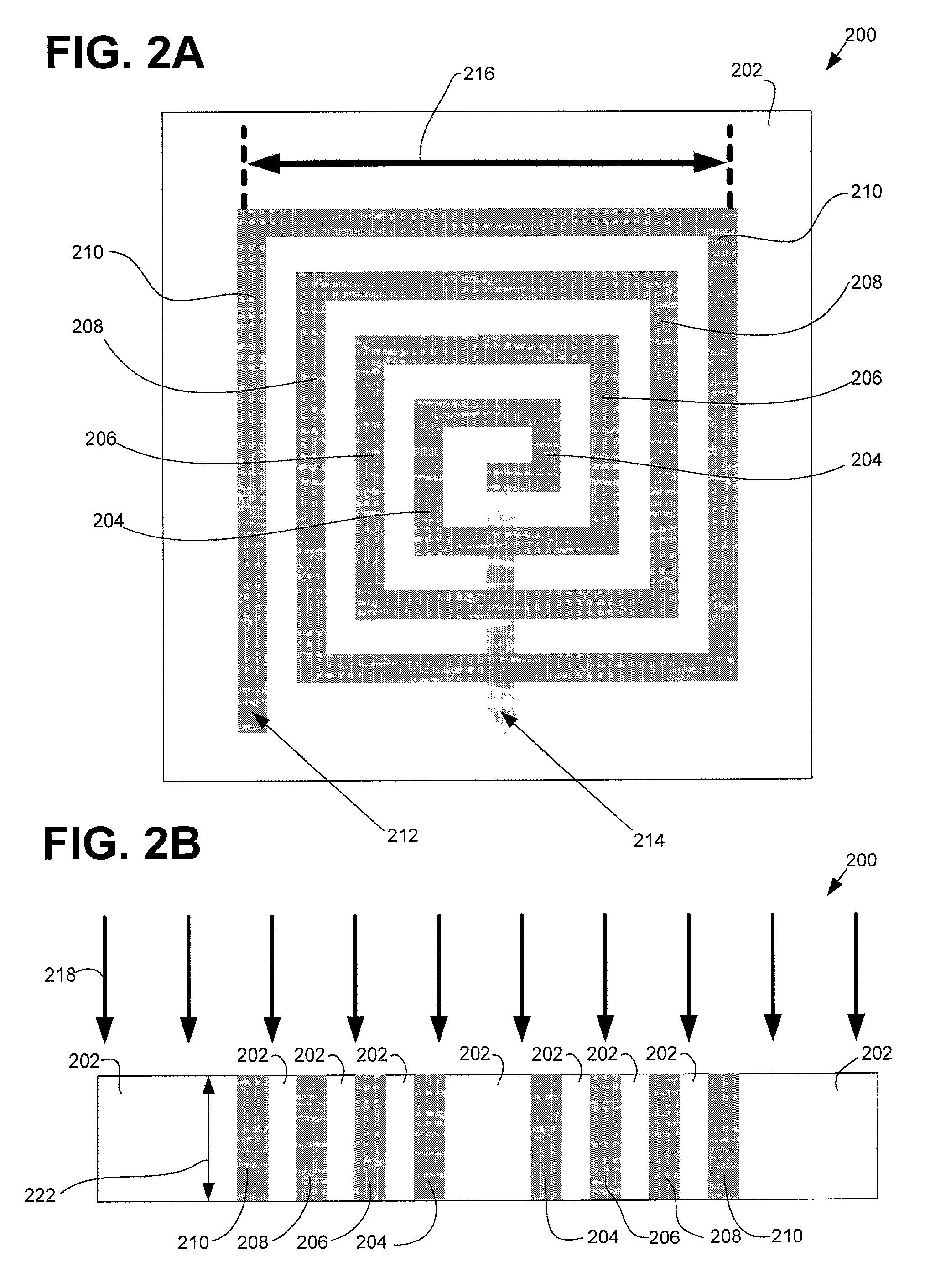
[0029]The present invention is method for fabrication of on-chip inductors and related structure. The following description contains specific information pertaining to different types of materials, layouts, dimensions, and implementations of the invention's inductor. One skilled in the art will recognize that the present invention may be practiced with material, layout, or dimensions different from those specifically discussed in the present application. Moreover, some of the specific details of the invention are not discussed in order to not obscure the invention. The specific details not described in the present application are within the knowledge of a person of ordinary skills in the art.

[0030]The drawings in the present application and their accompanying detailed description are directed to merely example embodiments of the invention. To maintain brevity, other embodiments of the invention which use the principles of the present invention are not specifically described in the p...


PUM


Abstract

Method for fabrication of on-chip inductors and related structure are disclosed. According to one embodiment, inductors are formed by patterning conductors within a certain dielectric layer in a semiconductor die. Thereafter, the entire dielectric layer in the semiconductor die is subjected to a blanket implantation or sputtering of high permeability material. According to another embodiment, a first area in a semiconductor die is covered, for example, with photoresist. A second area in the semiconductor die includes a patterned conductor which is to be used as an inductor. The patterned conductor is also covered, for example, with photoresist. The second area, excluding the covered patterned conductor, is subjected to implantation or sputtering of high permeability material. According to yet another embodiment, a first area of a semiconductor die is covered, for example, with photoresist. A second area in the semiconductor area includes a patterned conductor which is to be used as an inductor. This second area, including the patterned conductor, is subjected to implantation or sputtering of high permeability material. The implantation or sputtering of high permeability materials result in the inductors having much higher inductance values than they would otherwise have.

Description

[0001]This is a divisional of application Ser. No. 09 / 627,505 filed Jul. 28, 2000 now U.S. Pat. No. 6,309,922.BACKGROUND OF THE INVENTION[0002]1. Field of the Invention[0003]The present invention is generally in the field of semiconductor chips. In particular, the present invention is in the field of inductors used in semiconductor chips.[0004]2. Background Art[0005]FIG. 1 shows a top view of a conventional inductor 100 on an area of a semiconductor chip. The square configuration of the inductor shown in FIG. 1 is commonly used on semiconductor chips and is referred to as a “square spiral inductor.”[0006]The 4 metal turns of inductor 100 are referred to by numerals 104, 106, 108, and 110. Metal turns 104, 106, 108, and 110 are patterned within dielectric 102 in a manner known in the art. Thus, the areas of dielectric 102 which are flanked by metal turns 104, 106, 108, and 110 are within the electromagnetic field that will be created by metal turns 104, 106, 108, and 110. Dielectric ...

Claims


Application Information

Patent Timeline
IPC IPC(8): H01L29/00H01L21/02H01L27/08
CPCH01L28/10H01L27/08
Inventor LIU, Q ZZHAO, BINHOWARD, DAVID
Owner NEWPORT FAB
Why Eureka
Try Eureka