Low power clock distribution scheme

a clock distribution and low power technology, applied in the field of low power clock distribution in electronic circuits, can solve the problems of reducing reliability, reducing dynamic power consumption, and extremely low static power consumption, and achieve the effect of reducing power consumption

Inactive Publication Date: 2005-04-12
MINERAL LASSEN
View PDF10 Cites 28 Cited by
  • Summary
  • Abstract
  • Description
  • Claims
  • Application Information

AI Technical Summary

Benefits of technology

An embodiment of the invention provides an improved clock distribution architecture that reduces power consumption and prov

Problems solved by technology

The power consumption of an electronic circuit is largely dependant on the switching of the logic circuits in response to the clock signal because the static power consumption, especially for CMOS circuits that are widely used in electronic devices, is extremely low.
The predominant dynamic power consumption is the result of charging and discharging of internal and external capacitors.
Increased power dissipation also results in reduced reliability as the circuit

Method used


Image

  • Low power clock distribution scheme
  • Low power clock distribution scheme
  • Low power clock distribution scheme

Examples


Embodiment Construction

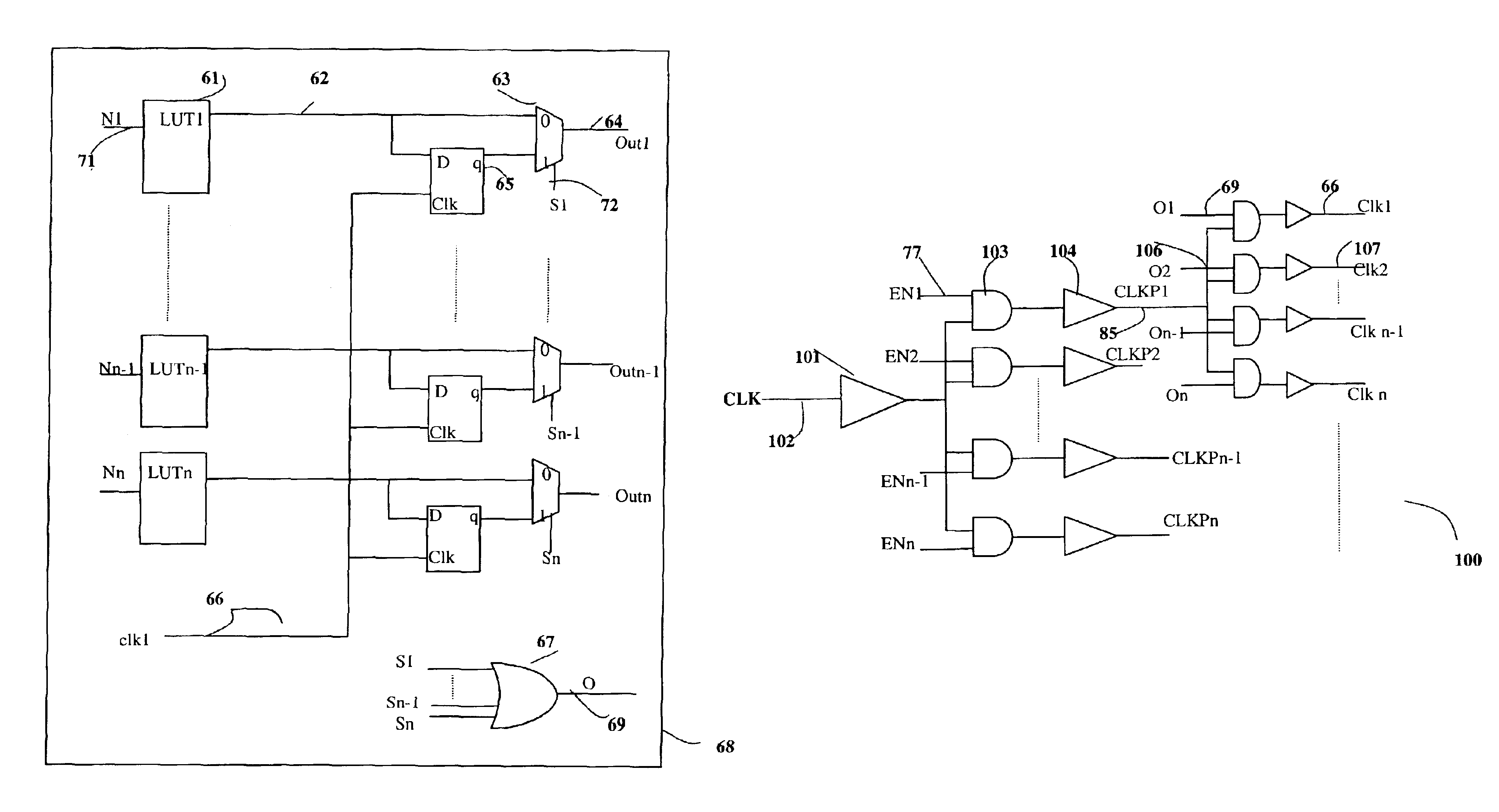
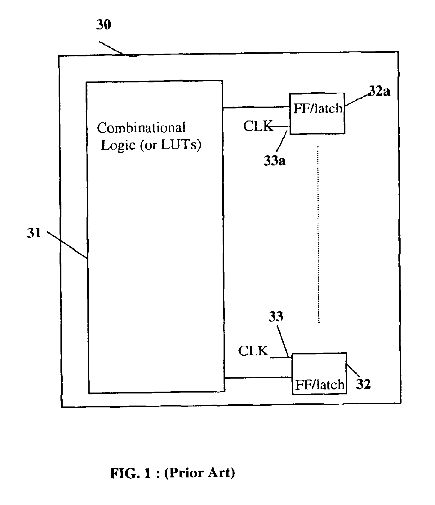
FIG. 1 shows the block diagram of a Programmable Logic Block (PLB) 30, of the type used in an FPGA, according to the prior art. The PLB contains one or more Look Up Tables (LUTs) 31 that define programmable, combinational-logic functions. The output of each LUT 31 is connected to a Flip Flop / Latch 32-32a. All the latches 32-32a in a PLB 30 share a common clock signal Clk 33-33a. Various combinational or sequential logic functions can be obtained by programming the LUT 31 suitably and selecting either the latched output or the combinational signal at the input of the latch 32-32a.

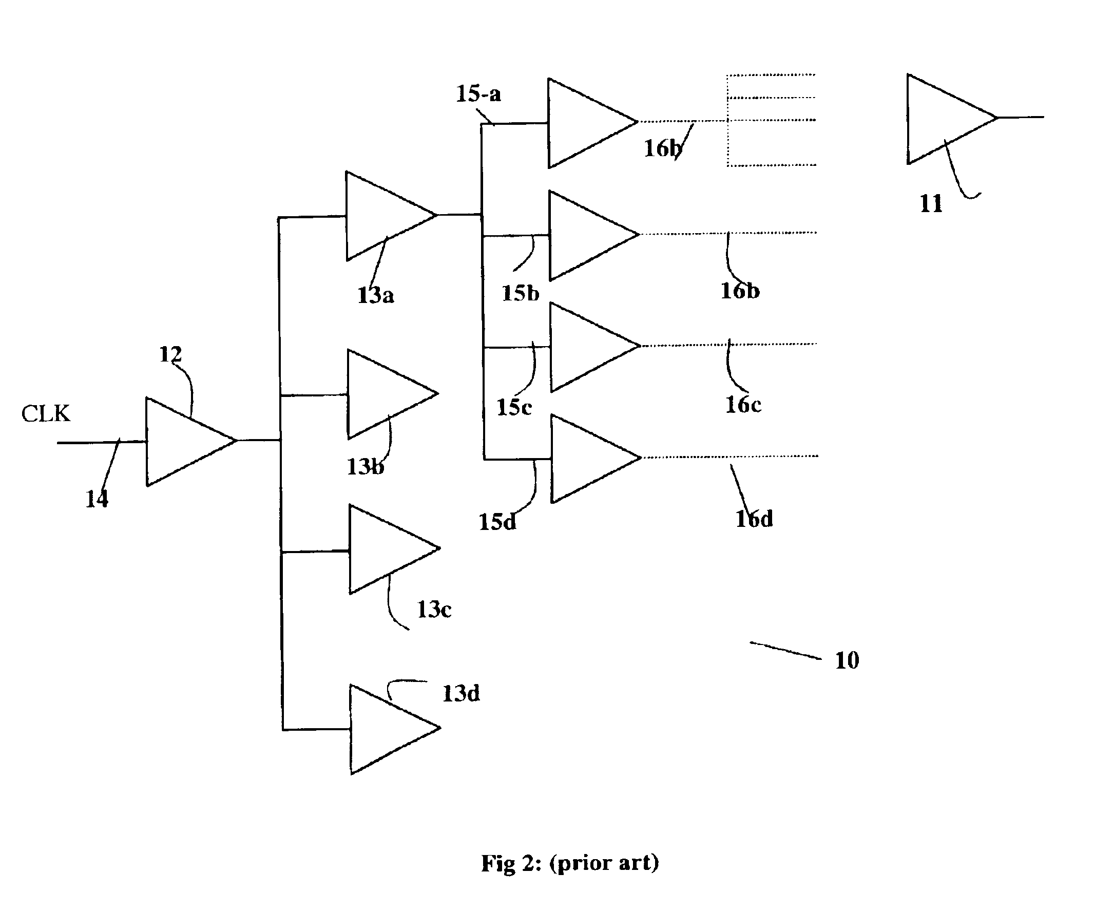
FIG. 2 shows a typical clock tree structure 10, according to prior art, used for supplying the clock signal to the PLBs. An external clock Clk 14 supplied to the entire device is buffered by buffer 12 and then distributed by first level distribution buffers 13a-13d. Each first level distribution buffer 13a-13d in turn supplies the clock signal to second level distribution buffers 15a-15d that supply the clo...


PUM


Abstract

An electronic circuit containing one or more digital synchronous sequential logic blocks at least one of which is either selected or deselected during operation. The electronic circuit includes an improved clock distribution scheme that reduces power consumption, comprising identifying means for determining the select/deselect state of each said deselectable synchronous sequential logic block, coupled to disabling means for disabling the clock input to each deselected synchronous sequential logic block.

Description

PRIORITYThis application claims priority from Indian patent application No. 431 / Del / 2002, filed Apr. 5, 2002, which is incorporated herein by reference.FIELD OF THE INVENTIONThe invention relates generally to clock distribution in electronic circuits. In particular, the invention relates to reduction of power consumption by selective enabling of clock signals.BACKGROUND OF THE INVENTIONA vast majority of digital electronic circuits include synchronous sequential logic circuits that require a clock signal for their operations. One or more clock signals are distributed to every part of the circuit containing such synchronous sequential logic circuits. For large circuits, it is a general practice to organize the clock distribution as a hierarchical arrangement in the form of a “clock tree” that distributes the clock over the entire circuit.The power consumption of an electronic circuit is largely dependant on the switching of the logic circuits in response to the clock signal because t...

Claims


Application Information

Patent Timeline
IPC IPC(8): H03K19/177
CPCH03K19/17784H03K19/1774
Inventor SWAMI, PARVESHKHANNA, NAMERITAAGARWAL, DEEPAK
Owner MINERAL LASSEN
Why Eureka
Try Eureka