Reflection type liquid crystal display provided with reflective layer, coplanar gate electrode, color filter layer and transparent pixel electrode and manufacture method thereof
- Summary
- Abstract
- Description
- Claims
- Application Information
AI Technical Summary
Benefits of technology
Problems solved by technology
Method used
Image
Examples
second embodiment
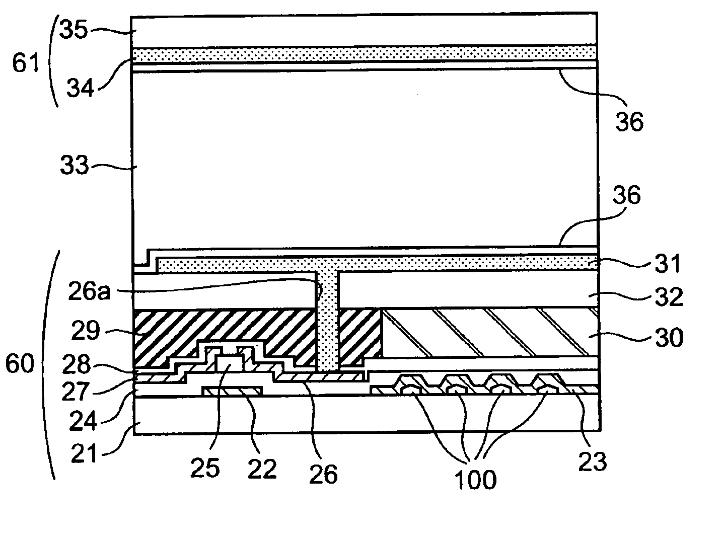
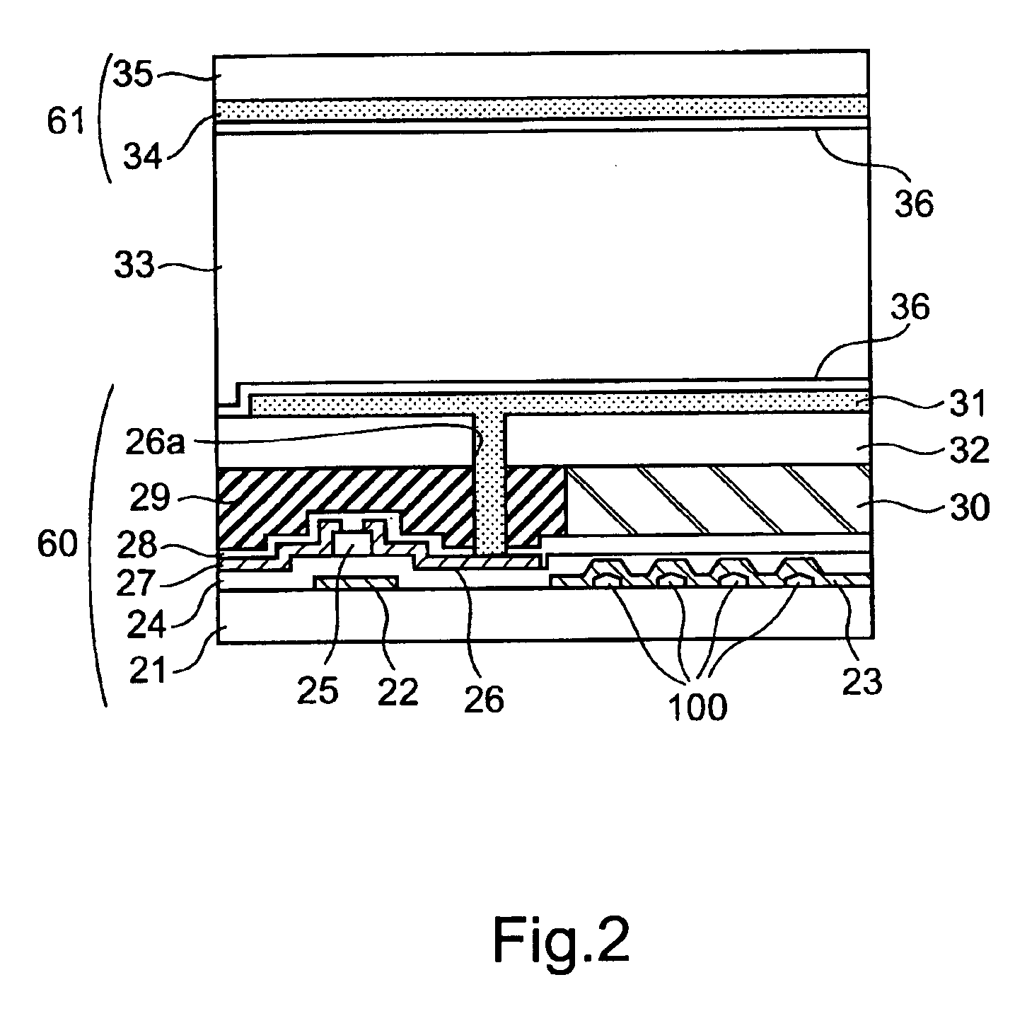
FIG. 2 is a sectional view showing the constitution of the liquid crystal display according to the present invention.
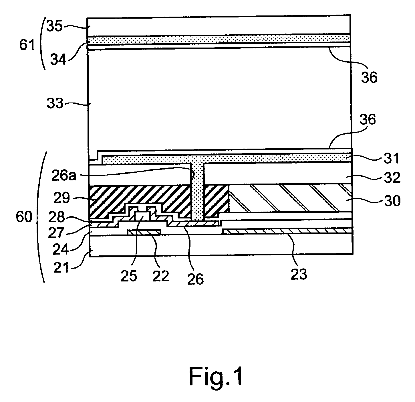
The liquid crystal display of the second embodiment is different from the liquid crystal display of the first embodiment in that concave / convex portions or rough portions 100 are formed on the first transparent insulation substrate 21. Except the formation of the rough portions 100, the liquid crystal display of the second embodiment has the same constitution as that of the liquid crystal display of the first embodiment.
As shown in FIG. 2, the rough portions 100 are formed on a first area of the substrate 21 located under the reflective layer 23. A second area of the substrate 21 is maintained as relatively smooth without any rough portions. The switching element that includes the gate electrode 22 is formed on the second area of the substrate 21.
The manufacture processes of the rough portions 100 or uneven portions will be described hereinafter. The manufacture proce...
third embodiment
FIG. 4 is a sectional view showing the constitution of the liquid crystal display according to the present invention.
In the reflection type liquid crystal display, the liquid crystal layer 33 is held between the thin film transistor substrate (TFT substrate) 60 on which the thin film transistor is formed and the opposite substrate 61.
For the TFT substrate 60, first, the gate electrode 22 is formed of aluminum or aluminum alloy such as aluminum-neodymium alloy on the first transparent insulation substrate 21 such as a glass plate, and the gate insulation film 24 is formed on the first transparent insulation substrate 21 to cover the gate electrode 22. Arranged above the gate electrode 22 are the semiconductor layer 25 formed on the gate insulation film 24, and the source electrode 26 and the drain electrode 27 formed in contact with the semiconductor layer 25 on the gate insulation film 24. The reflective layer 23 is formed integrally with the source electrode, and extends onto the g...
PUM
 Abstract
Description
Claims
Application Information


