Membrane probe with anchored elements

a technology of anchored elements and probes, applied in the field of probes, can solve problems such as electrical components failing

Inactive Publication Date: 2005-04-19
GLOBALFOUNDRIES INC
View PDF22 Cites 21 Cited by
  • Summary
  • Abstract
  • Description
  • Claims
  • Application Information

AI Technical Summary

Problems solved by technology

When a force is applied to the rivet from the test device and the electrical component, the rivet may tend to spin with

Method used


Image

  • Membrane probe with anchored elements
  • Membrane probe with anchored elements
  • Membrane probe with anchored elements

Examples


Embodiment Construction

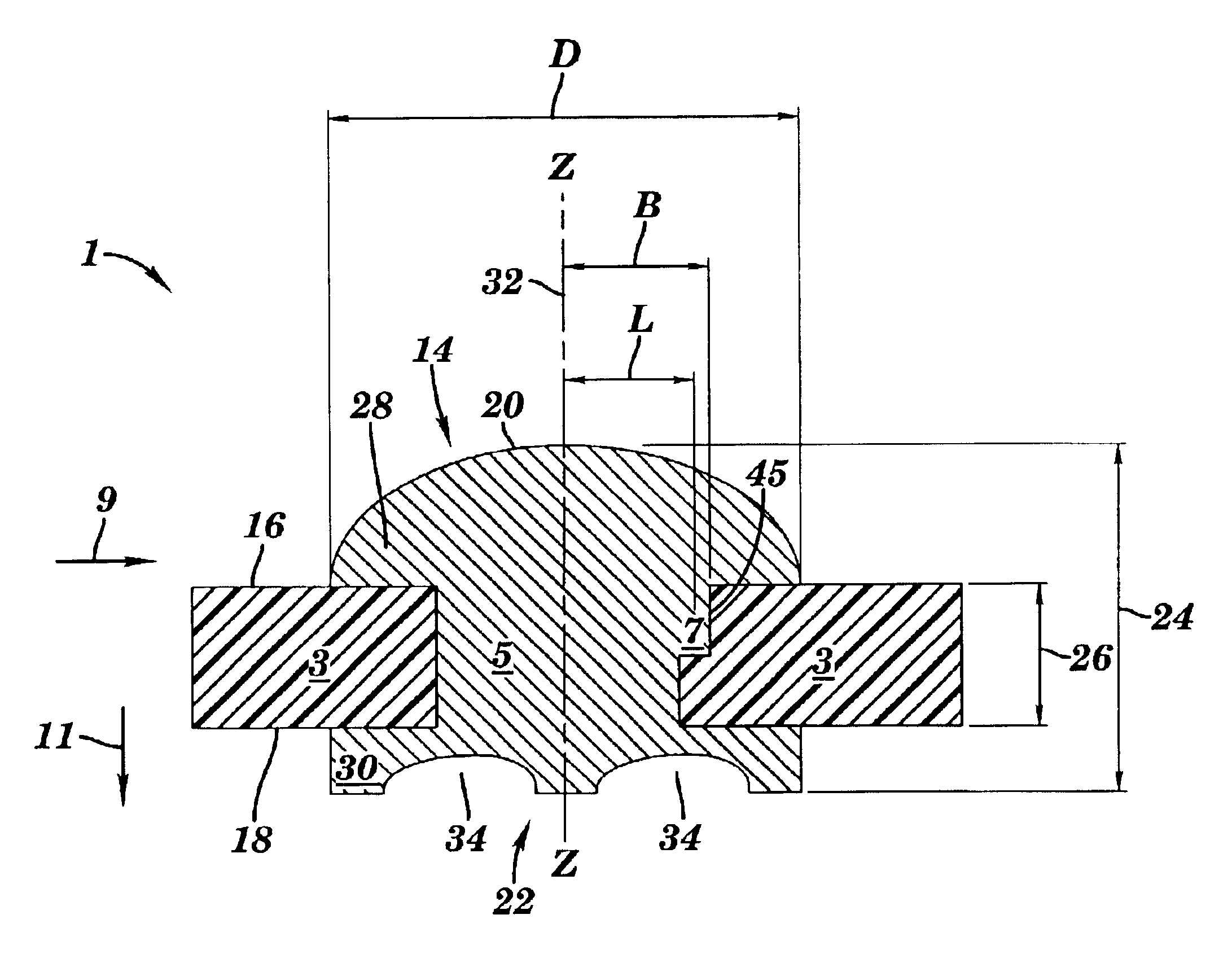
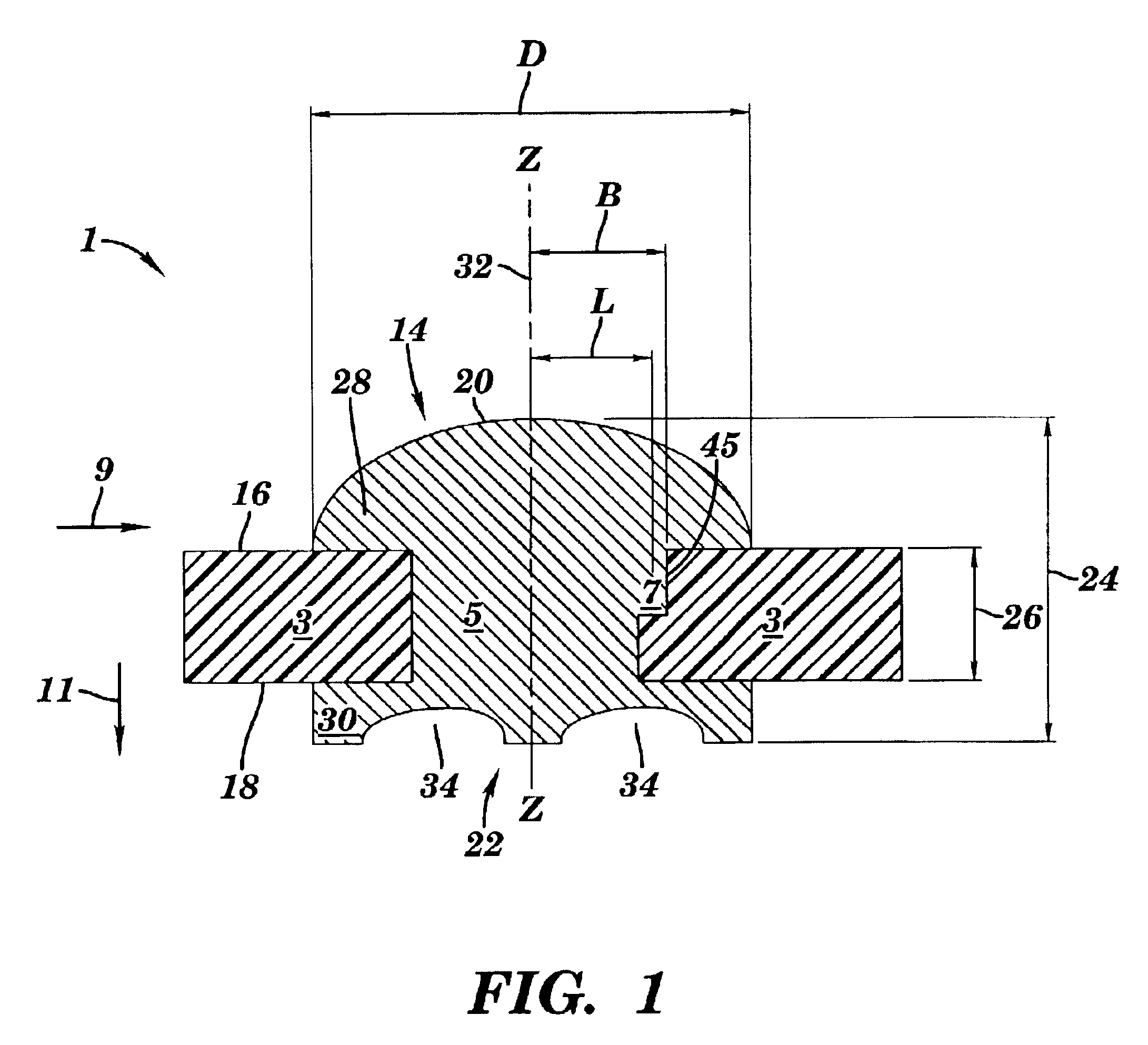
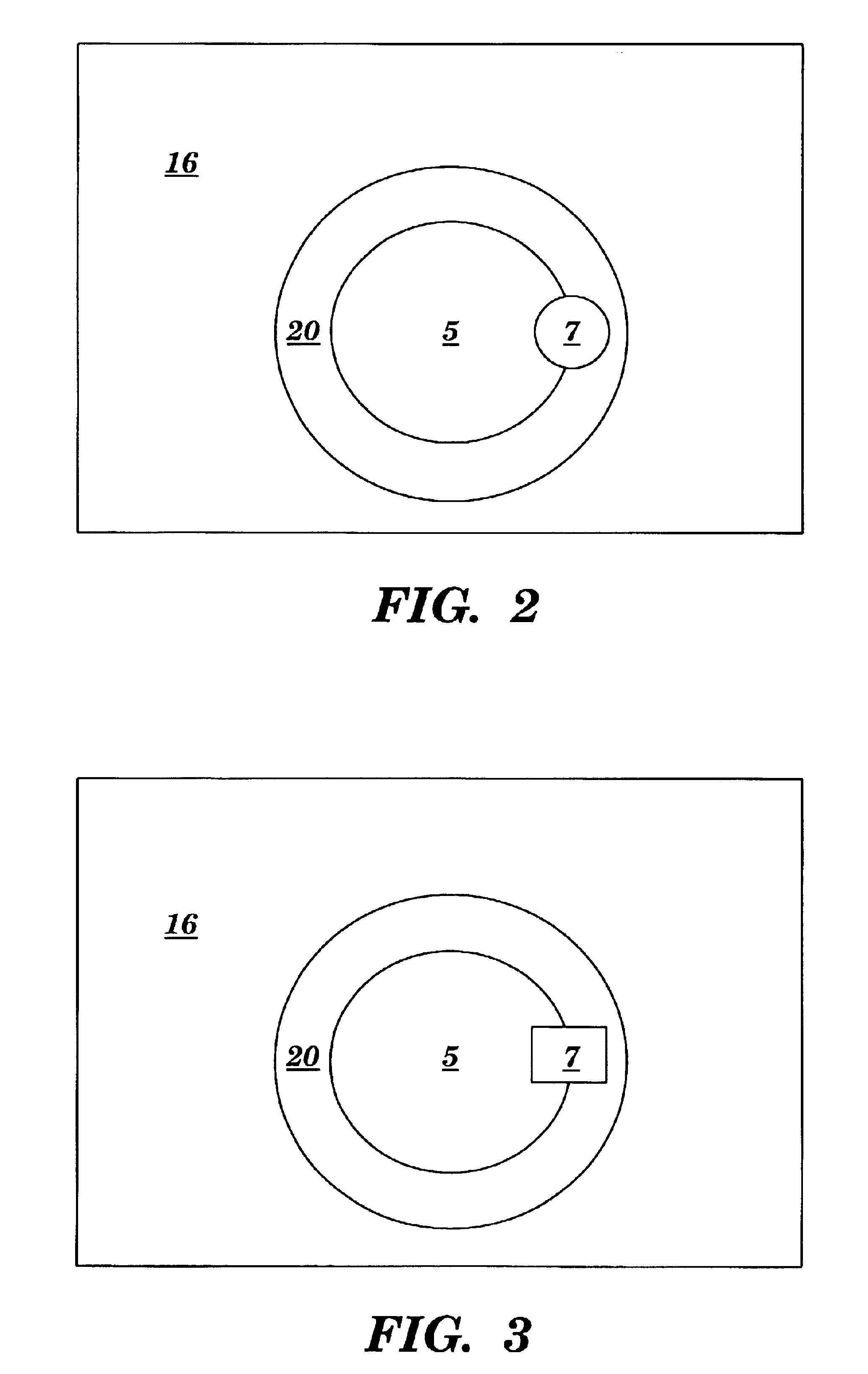
[0028]FIG. 1 illustrates a front cross sectional view of an electrical interconnection structure 1 comprising an electrically conductive member 14 having a first surface 20 and a second surface 22 extending through a first side 16 and a second side 18 of a flexible dielectric layer 3 to establish an electrical and mechanical connection between devices to be tested and a tester, in accordance with embodiments of the present invention. The electrical interconnection structure 1 may be a thin flexible interposer (TFI) membrane probe used for electrical testing of chips in a wafer format. The flexible dielectric layer 3 may be a polyimide (e.g., KAPTON®, etc). The flexible dielectric layer 3 may have a thickness in a range of about 0.5-2 mils. The flexible dielectric layer 3 comprises a through via 5 and a blind via 7. The via 5 and a blind via 7 may each have vertical sidewalls (i.e., parallel to the direction 11) or angular sidewalls (with respect to the direction 11). The through via...


PUM

PropertyMeasurementUnit
Electrical conductivityaaaaaaaaaa
Flexibilityaaaaaaaaaa

Abstract

A structure and method to establish an electrical connection between a tester and an electrical component. A flexible dielectric layer has a first side and a second side. A through via extends through the first side and the second side of the dielectric layer. A blind via is placed in a position that is offset from the through via and extends laterally in a first direction from a section of the first through via to a section of the flexible dielectric layer. The blind via extends in a second direction from the first side of the flexible dielectric layer to a section of the flexible dielectric layer that is between the first side and the second side of the dielectric layer. An electrically conductive member extends through the through via and extends into the blind via, thereby filling the through via and the blind via. The electrically conductive member has a first surface and a second surface. Any distance between the first surface and the second surface is greater than a distance between the first side of the dielectric layer and the second side of the dielectric layer.

Description

BACKGROUND OF THE INVENTION[0001]1. Technical Field[0002]The present invention relates to a probe used to establish an electrical connection between a test device and an electrical component.[0003]2. Related Art[0004]Probes used for establishing an electrical connection between a test device and an electrical component may consist of electrically conductive rivets within a dielectric material. These rivets are typically placed in a via within the dielectric material. When a force is applied to the rivet from the test device and the electrical component, the rivet may tend to spin within the via causing the rivet to electrically short to an adjacent via, thereby causing the electrical component to fail. Thus there is a need for preventing such failure.SUMMARY OF THE INVENTION[0005]The present invention provides an electrical interconnection structure, comprising:[0006]a flexible dielectric layer having a first side and a second side;[0007]a first through via extending through the fir...

Claims


Application Information

Patent Timeline
IPC IPC(8): G01R1/067H05K3/40H05K3/42G01R1/073H05K3/20
CPCG01R1/06733H05K3/4007H05K3/423H01R12/52Y10T29/4922H01R2201/20H05K3/205H05K2201/0367H05K2201/09745H05K2201/09845H05K2201/10378H05K2203/0369H05K2203/0733H01R12/7082H01R12/714G01R1/0735
Inventor EGITTO, FRANK D.MILLER, KEITH J.NGUYEN, MANH-QUAN T.
Owner GLOBALFOUNDRIES INC
Why Eureka
Try Eureka