pMOS device having ultra shallow super-steep-retrograde epi-channel with dual channel doping and method for fabricating the same

a metaloxide semiconductor and retrograde technology, applied in the direction of semiconductor devices, basic electric elements, electrical equipment, etc., can solve the problems of difficult to make the concentration difference between a maximum concentration and a maximum concentration, and the depth of the channel is required to be shallow. , to achieve the effect of high doping concentration

Inactive Publication Date: 2005-04-19
SK HYNIX INC
View PDF4 Cites 136 Cited by
  • Summary
  • Abstract
  • Description
  • Claims
  • Application Information

AI Technical Summary

Problems solved by technology

However, as a channel length decreases, a channel depth is required to be shallow.
Thus, a typical ion implantation method has a limitation in realization of a retrograde channel of which channel depth is below about 50 nm.
That is, it is difficult to make the concentration difference between a maximum concentration (Cmax) of the epi-channel and a concentration of a silicon surface (Cs) above 30 times. It is also difficult to provide the Cmax of the epi-channel above 3×10¹⁸ atoms / cm3.
These facts result in a further disadvantage of forming the epi-channel able to prevent a short channel phenomenon in a MOSFET device of which gate length is less than 70 nm.
Despite of this advantage, a dopant concentration of an epi-channel is too low due to a low diffusion rate of the dopant, further resulting in a low threshold voltage and a subsequent problem of excessive sub-threshold leakages at below the threshold voltage.

Method used


Image

  • pMOS device having ultra shallow super-steep-retrograde epi-channel with dual channel doping and method for fabricating the same
  • pMOS device having ultra shallow super-steep-retrograde epi-channel with dual channel doping and method for fabricating the same
  • pMOS device having ultra shallow super-steep-retrograde epi-channel with dual channel doping and method for fabricating the same

Examples


Embodiment Construction

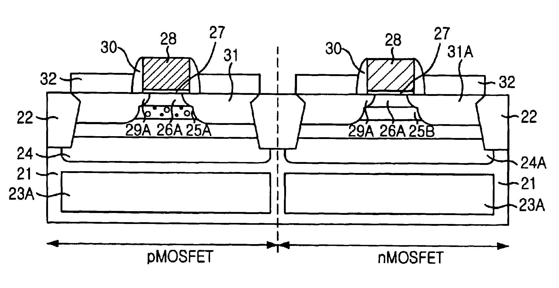
[0030]FIG. 3 is a cross-sectional view of a p-channel metal-oxide-semiconductor field effect transistor (pMOSFET) having an ultra shallow super-steep-retrograde epi-channel in accordance with a first preferred embodiment of the present invention.

[0031]As shown, a gate insulating layer 27 and a gate electrode 28 are formed on a semiconductor substrate 21 in which an n-type well 23 and an n-type field punchthrough-stop layer 24 are formed. An epi-channel including a silicon epi-layer 26 and an n-type p-channel doping layer 25A is formed in the semiconductor substrate beneath the gate insulating layer 27. Afterwards, a highly concentrated p-type source / drain extension (SDE) region 29 is formed at both lateral sides of the epi-channel, and a highly concentrated p-type source / drain (SD) region 31 electrically connected to the p-type SDE region 29 is subsequently formed thereafter. A spacer 30 is formed at both lateral sides of the gate electrode 28.

[0032]In FIG. 3, the n-type p-channel d...


PUM


Abstract

The present invention provides a p-channel metal-oxide-semiconductor (pMOS) device having an ultra shallow epi-channel satisfying a high doping concentration required for a device of which gate length is about 30 nm even without using a HALO doping layer and a method for fabricating the same. The pMOS device includes: a semiconductor substrate; a channel doping layer being formed in a surface of the semiconductor substrate and being dually doped with dopants having different diffusion rates; a silicon epi-layer being formed on the channel doping layer, whereby constructing an epi-channel along with the channel doping layer; a gate insulating layer formed on the silicon epi-layer; a gate electrode formed on the gate insulating layer; a source / drain extension region highly concentrated and formed in the semiconductor substrate of lateral sides of the epi-channel; and a source / drain region electrically connected to the source / drain extension region and deeper than the source / drain region.

Description

RELATED APPLICATION DATA[0001]This application claims the benefit of foreign priority under 35 U.S.C. §119 of Korean patent application number 2002-0086275 filed Dec. 30, 2002.[0002]1. Field of the Invention[0003]The present invention relates to a method for fabricating a p-channel metal-oxide semiconductor (pMOS) device; and, more particularly, to a p-channel metal-oxide-semiconductor field effect transistor (pMOSFET) having an ultra shallow super-steep-retrograde epi-channel of which gate length is below 100 nm and a method for fabricating the same.[0004]2. Description of Related Arts[0005]Generally, in a metal-oxide-semiconductor field effect transistor (MOSFET) or a metal-insulator-semiconductor field effect transistor (MISFET), a surface region of a semiconductor substrate below a gate electrode and a gate oxide layer acts to flow currents by using an electric field supplied to a source / drain in a state that voltage is supplied to the gate electrode, and this surface region is ...

Claims


Application Information

Patent Timeline
Patent Type & Authority Patents(United States)
IPC IPC(8): H01L21/265H01L21/70H01L29/66H01L29/10H01L29/78H01L21/02H01L29/02H01L21/324H01L21/8238
CPCH01L21/26513H01L21/324H01L29/7833H01L21/823842H01L29/1033H01L21/823807H01L21/2658H01L29/78
Inventor SOHN, YONG-SUN
Owner SK HYNIX INC
Why Eureka
Try Eureka