Use of amorphous carbon hard mask for gate patterning to eliminate requirement of poly re-oxidation

a technology of amorphous carbon and mask, which is applied in the direction of basic electric elements, electrical apparatus, semiconductor devices, etc., can solve the problems of low melting point, difficult etching of metal gate conductors, and less compatibility with front-end processing

Inactive Publication Date: 2005-04-26
ADVANCED MICRO DEVICES INC
View PDF22 Cites 87 Cited by
  • Summary
  • Abstract
  • Description
  • Claims
  • Application Information

AI Technical Summary

Problems solved by technology

Conventional processes typically utilize polysilicon based gate conductors because metal gate conductors are difficult to etch, are less compatible with front-end processing, and have relatively low melting points.
One issue that must be considered in fabricating integrated circuits is damage to gate structures resulting from the removal of etch masks overlying the gate structure.
Damage to the gate structures is particularly pronounced for n-type doped gates.
One difficulty with a poly-reoxidation step to form an oxide layer on the side of the gate structures is that polysilicon re-oxidation is performed at an elevated temperature that increases the thermal budget of processing.
Another difficulty is that the oxide formed on the sides of the gate structures during the polysilicon re-oxidation is not localized on the sides of the gate structures, but extends to a point near the thin gate oxide layer underlying the gate conductor material.
The newly-formed oxide may encroach into the gate oxide layer, which may adversely increase the thickness of the gate oxide or reduce the shape definition of the corner between the gate structure and the underlying substrate.
Thus, the polysilicon re-oxidation may affect the precision with which gate structures may be formed.
Even further still, there is a need to form gate structures without the use of a polysilicon re-oxidation process that may result in damage to the gate oxide and adversely affect definition of the gate structure.

Method used


Image

  • Use of amorphous carbon hard mask for gate patterning to eliminate requirement of poly re-oxidation
  • Use of amorphous carbon hard mask for gate patterning to eliminate requirement of poly re-oxidation
  • Use of amorphous carbon hard mask for gate patterning to eliminate requirement of poly re-oxidation

Examples


Embodiment Construction

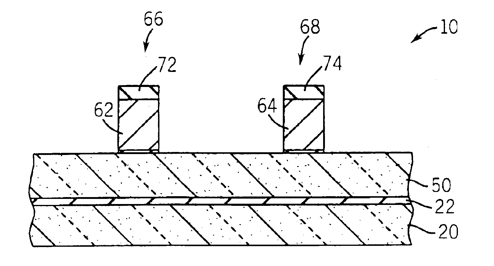
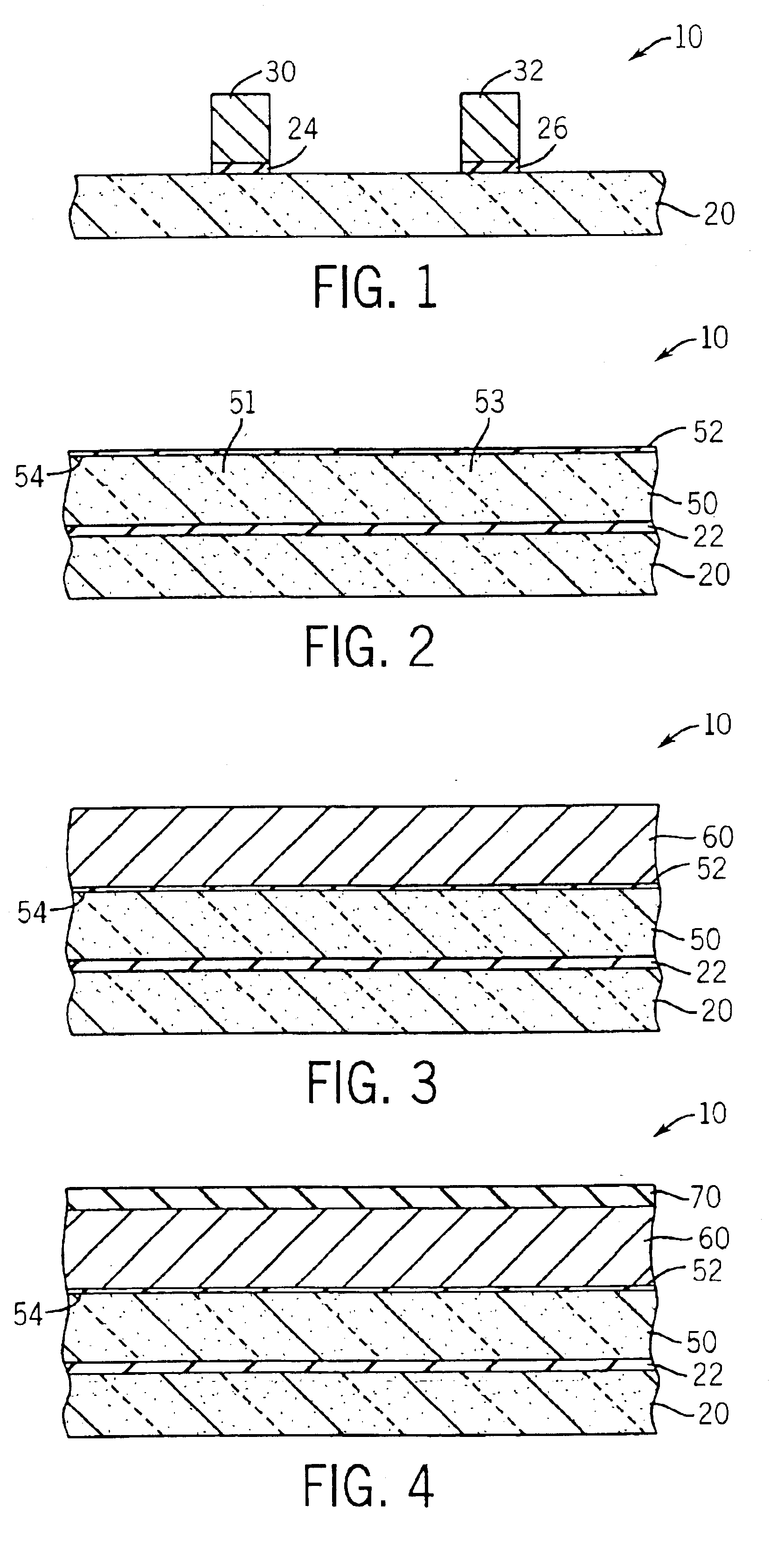
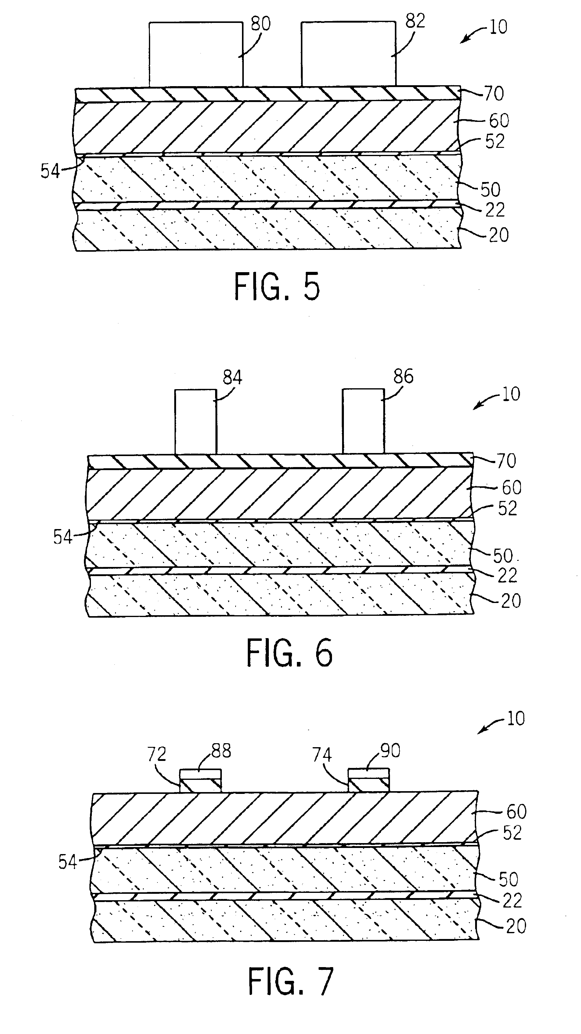
[0026]Referring to FIG. 1, a portion 10 of an integrated circuit (IC) includes a substrate 20 (e.g. a silicon wafer), line or gate conductors 30, 32, and oxide layers 24, 26. Oxide layers 24, 26 may be referred to as gate oxide layers. Portion 10 is preferably part of an ultra-large-scale integrated (ULSI) circuit having a million or more transistors, and is manufactured as part of the IC on a wafer made of a semiconducting material (e.g., silicon, gallium arsenide, etc.).

[0027]Gate conductors 30, 32 can be a polysilicon or polysilicon / germanium (SixGe(1-x)) material that controls charge carriers in a channel region formed between source and drain regions in substrate 20 to turn the transistor on and off. Gate conductors 30, 32 may be doped or undoped. In an exemplary embodiment, gate conductors 30, 32 are made of a polysilicon material that is doped with n-type (e.g., phosphorous) or p-type (e.g., boron) dopants and have a thickness between approximately 1000 and 2000 angstroms and...


PUM

PropertyMeasurementUnit
widthaaaaaaaaaa
widthaaaaaaaaaa
thicknessaaaaaaaaaa

Abstract

A method of producing an integrated circuit eliminates the need to re-oxidize polysilicon gate conductors and lines prior to removal of a hard mask used to form the gate conductors. A layer of polysilicon is provided above a semiconductor substrate. The layer of polysilicon is then doped. A mask material comprising amorphous carbon is provided above the layer of polysilicon, and the layer of mask material is patterned to form a mask. A portion of the layer of polysilicon is removed according to the mask, and the mask is removed.

Description

CROSS-REFERENCE TO RELATED PATENT APPLICATIONS[0001]This application is related to U.S. patent application Ser. No. 10 / 230,775 entitled “Use of Buffer Dielectric Layer with Amorphous Carbon Mask to Reduce Line Warpage,” U.S. patent application Ser. No. 10 / 277,760 entitled “Sacrificial Air Gap Layer for Insulation of Metals,” U.S. patent application Ser. No. 10 / 244,650 entitled “Use of Multilayer Amorphous Carbon Hard Mask to Eliminate Line Warpage Phenomenon,” U.S. patent application Ser. No. 10 / 424,420 entitled “Use of Amorphous Carbon for Gate Patterning,” U.S. patent application Ser. No. 10 / 230,794 entitled “Formation of Amorphous Carbon ARC Stack Having Graded Transition Between Amorphous Carbon and ARC Material,” U.S. patent application Ser. No. 10 / 335,726 entitled “Use of Diamond as a Hard Mask Material,” U.S. patent application Ser. No. 10 / 424,675 entitled “Selective Stress-Inducing Implant and Resulting Pattern Distortion in Amorphous Carbon Patterning,” U.S. patent applicat...

Claims


Application Information

Patent Timeline
Patent Type & Authority Patents(United States)
IPC IPC(8): H01L21/02H01L21/033H01L21/3213H01L21/28
CPCH01L21/0332H01L21/32139H01L21/0337H01L21/28123
Inventor DAKSHINA-MURTHY, SRIKANTESWARABELL, SCOTT A.BROWN, DAVID E.FISHER, PHILIP A.
Owner ADVANCED MICRO DEVICES INC
Why Eureka
Try Eureka