

Semiconductor device in which occurrence of slips is suppressed
a technology of semiconductor devices and sleeve, which is applied in the direction of semiconductor devices, electrical devices, transistors, etc., can solve the problems of difficult to form a satisfactory device, risk of slipping in the supporting portion of the substrate, and the peripheral portion of the rear surface of the substra
- Summary
- Abstract
- Description
- Claims
- Application Information
AI Technical Summary
Benefits of technology
Problems solved by technology
Method used
Image

Examples
first embodiment
[0033](First Embodiment)
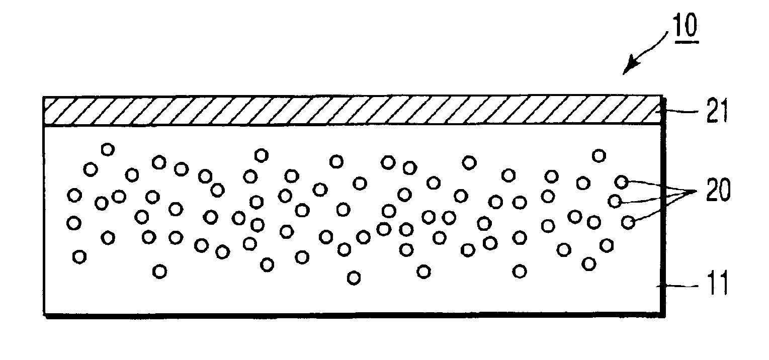
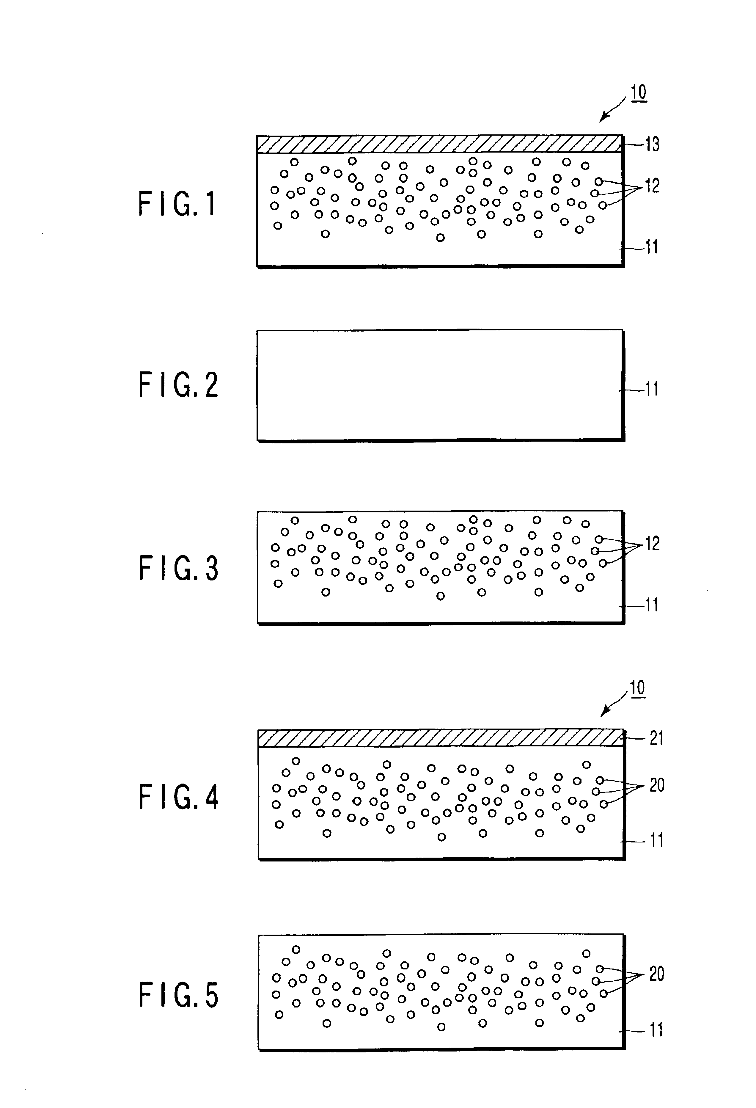
[0034]FIG. 1 shows a semiconductor device 10 according to a first embodiment of the invention. The semiconductor device 10 includes a silicon substrate 11 having an oxygen precipitation layer 12 formed therein. For example, the substrate 11 is a high-resistance substrate having a resistance of 1000Ω or more.
[0035]A silicon layer 13 is formed on the surface of the substrate 11. The silicon layer 13 has a dissolved oxygen concentration of 8×10¹⁷ atoms / cm3 or less and an impurity concentration of 1×10¹⁵ atoms / cm3 or less. Since the dissolved oxygen concentration is less than or equal to 8×10¹⁷ atoms / cm3, the silicon layer 13 has a high resistance of 1000Ω or more, like the substrate 11. The film thickness of the silicon layer 13 is 1 μm to 10 μm, for example. The film thickness of the silicon layer 13 may be selectively set according to the depth of the device to be formed and the distance from the oxygen precipitation layer 12 to the bottom of the device, and i...
second embodiment
[0043](Second Embodiment)
[0044]FIGS. 4 and 5 show a second embodiment of the invention.
[0045]In the semiconductor device 10 shown in FIG. 4, for example, a silicon substrate 11 contains an impurity 20 such as carbon which does not act as an acceptor or donor for the silicon. The concentration of carbon is 1×10¹⁶ atoms / cm3 or more, for example, and preferably 5×10¹⁷ atoms / cm3 or more. Further, the concentration of dissolved oxygen in the substrate 11 is 8×10¹⁷ atoms / cm3 or less, for example, and the concentration of an impurity which acts as an acceptor or donor is 1×10¹⁵ atoms / cm3 or less, for example. Since the concentration of dissolved oxygen in the substrate 11 is less than or equal to 8×10¹⁷ atoms / cm3, the substrate 11 has a high resistance of 1000Ω, for example.
[0046]A silicon layer 21 is formed on the substrate 11. For example, the silicon layer 21 contains carbon at a concentration of 1×10¹⁷ atoms / cm3 or less, dissolved oxygen at a concentration of 8×10¹⁷ atoms / cm3 or less, ...
third embodiment
[0052](Third Embodiment)
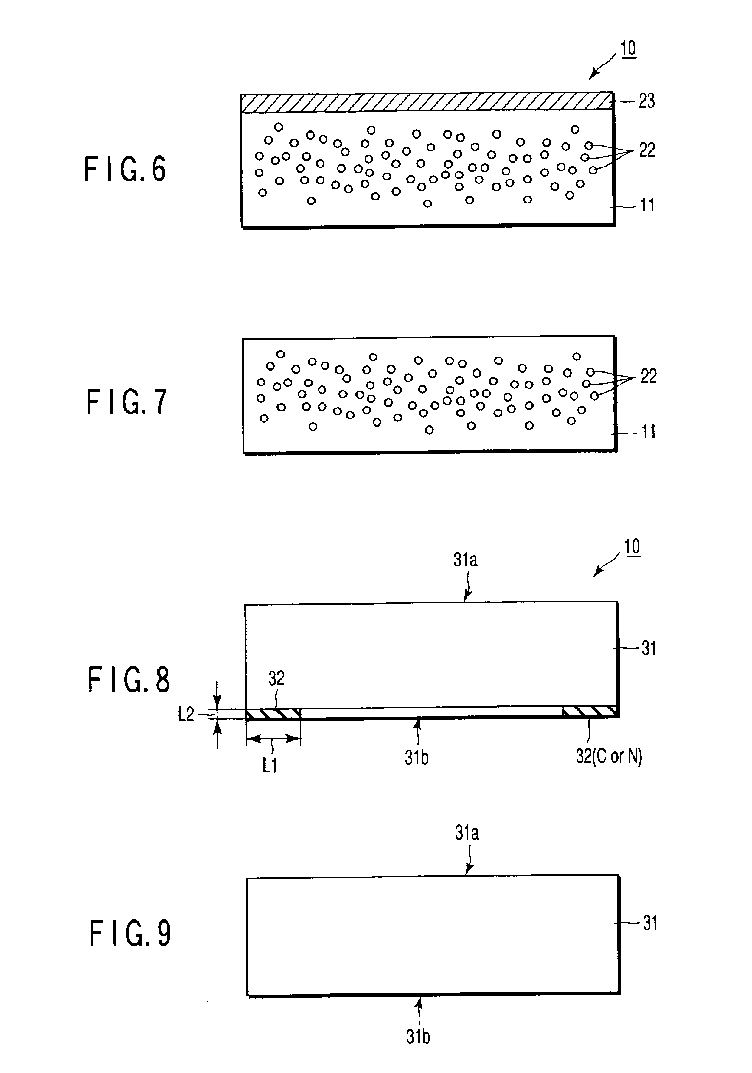
[0053]FIGS. 6 and 7 show a third embodiment of the invention. While, in the second embodiment, the substrate 11 contains carbon, in the third embodiment, the substrate 11 contains nitrogen.
[0054]In the semiconductor device 10 shown in FIG. 6, for example, the silicon substrate 11 contains an impurity 22 such as nitrogen which does not acts as an acceptor or donor for silicon. The concentration of nitrogen is 5×10¹³ atoms / cm3 or more. Further, the dissolved oxygen concentration in the substrate 11 is 8×10¹⁷ atoms / cm3 or less, for example, and the concentration of an impurity which is used as an acceptor or donor is 1×10¹⁵ atoms / cm3 or less, for example. Since the concentration of dissolved oxygen in the substrate 11 is less than or equal to 8×10¹⁷ atoms / cm3, the substrate 11 has a high resistance of 1000Ω or more, for example.
[0055]A silicon layer 23 is formed on the substrate 11. For example, the silicon layer 23 contains nitrogen having a concentration of 5×...
PUM
 Abstract
Description
Claims
Application Information