
Process for preparing single crystal silicon having improved gate oxide integrity

a single crystal silicon and integrity technology, applied in the field of single crystal silicon ingot preparation, can solve the problems of high production cost, high production cost, and inability to produce single crystal silicon of acceptable quality, and achieve the highest possible pull rate, improve gate oxide integrity, and maximize throughput and yield

Inactive Publication Date: 2005-07-28
GLOBALWAFERS CO LTD
View PDF17 Cites 5 Cited by
  • Summary
  • Abstract
  • Description
  • Claims
  • Application Information

AI Technical Summary

Benefits of technology

[0011] Among the several features of the present invention therefore is the provision of a single crystal silicon ingot, from which a single crystal silicon wafer may be obtained, having improved gate oxide integrity, and a process for the preparation thereof; the provision of such a process wherein the highest possible pull rates, for a given crystal puller, can be employed, thus maximizing throughput and yield; the provision of such a process wherein growth conditions are controlled to limit the size of agglomerated vacancy defects formed; the provision of such a process wherein the density of agglomerated vacancy defects is controlled; and, the provision of such a process wherein the residual vacancy concentration is limited to avoid uncontrolled oxygen precipitation.

Problems solved by technology

In recent years, it has been recognized that a number of defects in single crystal silicon form in the growth chamber as the ingot cools from the temperature of solidification.
Upon cooling to below this threshold temperature, a reaction or agglomeration event occurs, resulting in the formation of agglomerated intrinsic point defects.
However, until now, there has generally been no clear way to produce single crystal silicon of an acceptable quality using such growth conditions.
For example, high pull rates / cooling rates typically mean a high vacancy concentration, which leads to a high concentration of small, agglomerated defects.
However, such conditions are also unfavorable because they have traditionally been considered to yield wafers having poor gate oxide integrity.
In contrast, when slower pull rates / cooling rates are employed as a means by which to improve GOI (slow cooling typically resulting in a few, very large agglomerated vacancy defects being formed), the resulting size of LPDs is unacceptable.
More specifically, high pull rates typically lead to high vacancy concentrations in the silicon that is formed, and well as high cooling rates.
High cooling rates, in turn, typically lead to a high residual vacancy concentration (i.e., the concentration of silicon lattice vacancies present in the silicon, once it has cooled to a temperature at which vacancies are essentially no longer mobile).
High residual vacancy concentrations are problematic because, upon subsequent heating, they can lead to uncontrolled oxygen precipitation.

Method used


Image

  • Process for preparing single crystal silicon having improved gate oxide integrity
  • Process for preparing single crystal silicon having improved gate oxide integrity
  • Process for preparing single crystal silicon having improved gate oxide integrity

Examples


Embodiment Construction

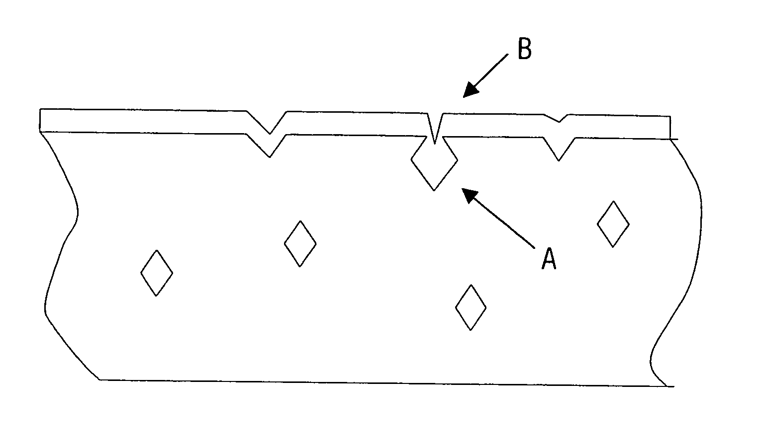
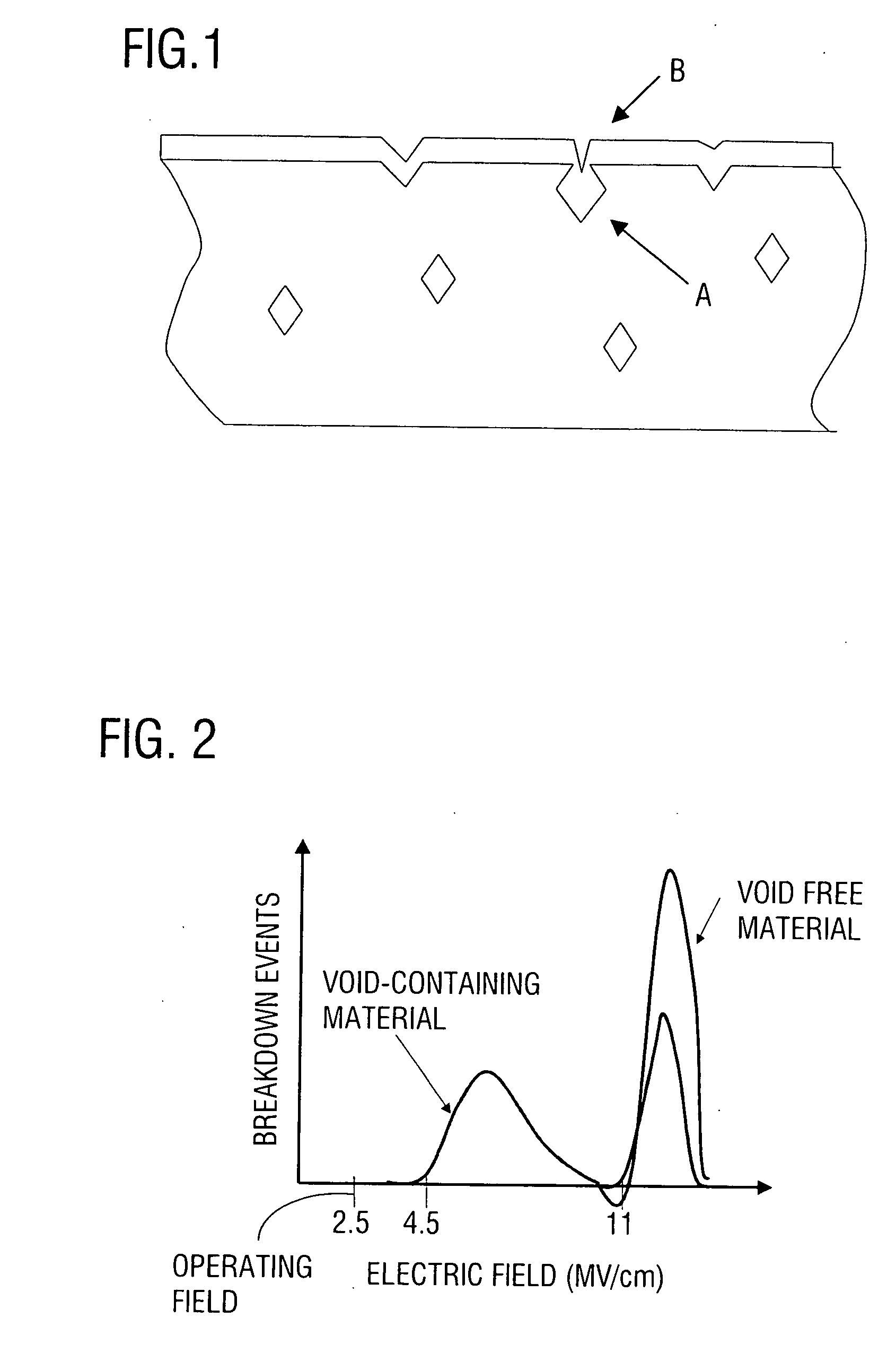
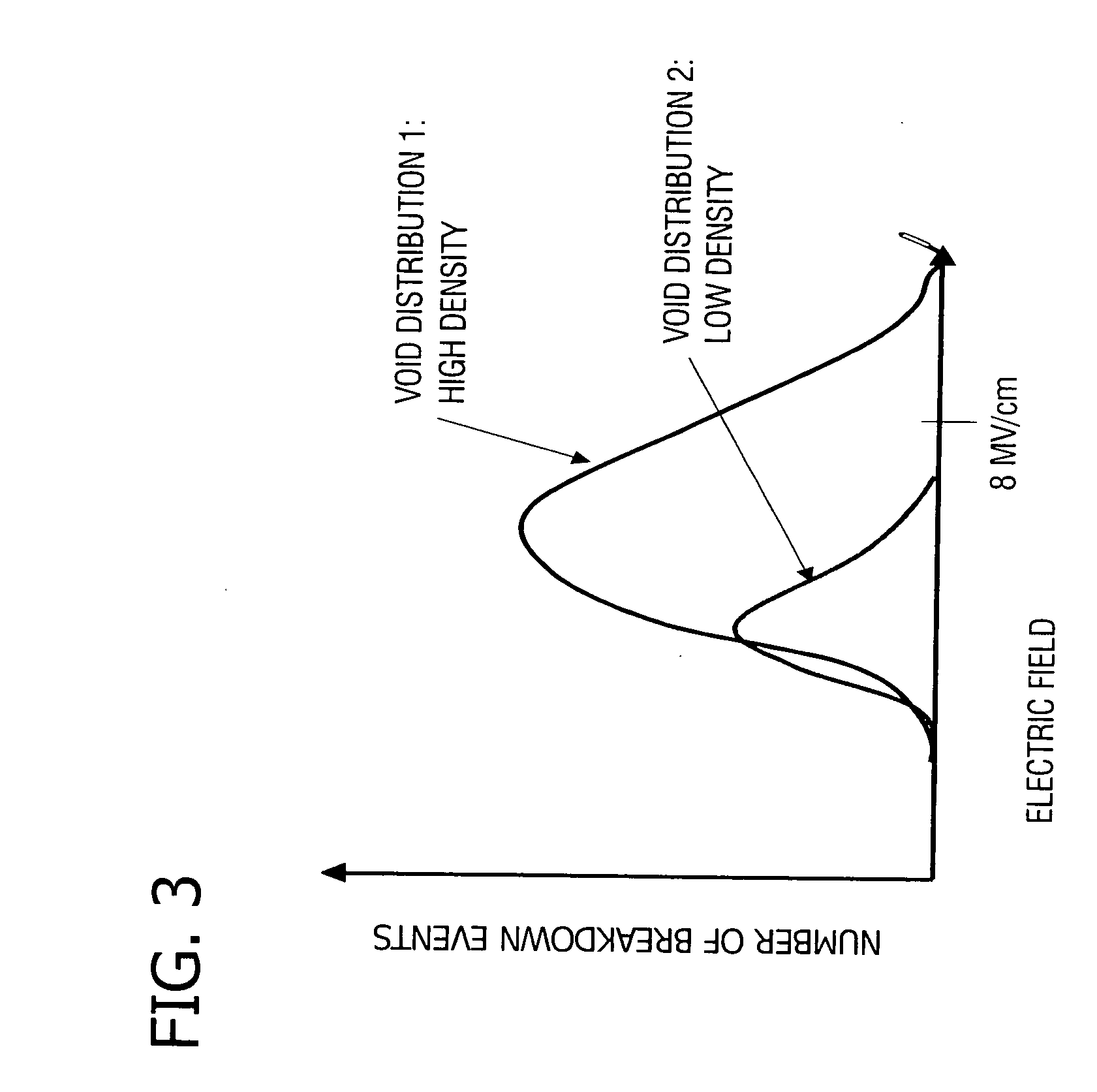
[0038] Based upon experimental evidence to-date, it appears that presently accepted practices for determining gate oxide integrity in single crystal silicon wafers are inaccurate and, as a result, lead to the disposal and therefore waste of wafers which would otherwise be acceptable for use. More specifically, gate oxide integrity requirements are typically presented in terms of a percent failure at a given electrical field, a field which is substantially greater than the field at which the integrated circuit will be operated (e.g., 2×, 3×, 4×, etc. the operating field). As further explained below, such tests can and, it is now believed, do result in the rejection of material which is acceptable for use. This waste is primarily the result of a test which erroneously leads to the conclusion that a few, large agglomerated defects in a given wafer are preferable to a number of, in comparison, relatively small defects.

[0039] Accordingly, the present invention enables more wafers to be ...


PUM

PropertyMeasurementUnit
diameteraaaaaaaaaa
average radiusaaaaaaaaaa
lengthaaaaaaaaaa

Abstract

A process for producing a single crystal silicon wafer comprising a front surface, a back surface, a lateral surface joining the front and back surfaces, a central axis perpendicular to the front and back surfaces, and a segment which is axially symmetric about the central axis extending substantially from the front surface to the back surface in which crystal lattice vacancies are the predominant intrinsic point defect, the segment having a radial width of at least about 25% of the radius and containing agglomerated vacancy defects and a residual concentration of crystal lattice vacancies wherein (i) the agglomerated vacancy defects have a radius of less than about 70 nm and (ii) the residual concentration of crystal lattice vacancy intrinsic point defects is less than the threshold concentration at which uncontrolled oxygen precipitation occurs upon subjecting the wafer to an oxygen precipitation heat treatment.

Description

REFERENCE TO RELATED APPLICATION [0001] This is a division of application Ser. No. 10 / 039,196, filed Jan. 2, 2002, which claims the benefit of U.S. Provisional Application No. 60 / 259,362, filed Jan. 2, 2001, both of which are incorporated in their entirety herein by reference.BACKGROUND OF THE INVENTION [0002] In general, the present invention relates to the preparation of a single crystal silicon ingot according to the Czochralski method. In particular, the invention relates to a high throughput process for preparing single crystal silicon wafers having improved gate oxide integrity, wherein the growth conditions of a single crystal silicon ingot, from which the wafers are derived, are controlled. More specifically, the growth conditions of a single crystal silicon ingot, including the growth velocity, the average axial temperature gradient and the cooling rate, are controlled in order to limit the size, and in some cases the density, of vacancy-related agglomerated defects, and op...

Claims


Application Information

Patent Timeline
Patent Type & Authority Applications(United States)
IPC IPC(8): C30B29/06C30B15/00C30B15/20C30B33/02H01L21/26
CPCC30B15/203Y10T428/21C30B29/06C30B15/206
Inventor FALSTER, ROBERT J.VORONKOV, VLADIMIR V.MUTTI, PAOLOBONOLI, FRANCESCO
Owner GLOBALWAFERS CO LTD
Learn More