Semiconductor laser device

a laser device and semiconductor technology, applied in the direction of semiconductor laser structural details, lasers, semiconductor lasers, etc., can solve the problems of poor heat rejection of resin molding packages, unstable reference surfaces for positioning, and above-mentioned improvement to achieve better heat dissipation and mechanical strength, stable reference surfaces, and high fitting accuracy.

Inactive Publication Date: 2005-04-26
SANYO ELECTRIC CO LTD +1
View PDF13 Cites 15 Cited by
  • Summary
  • Abstract
  • Description
  • Claims
  • Application Information

AI Technical Summary

Benefits of technology

[0013]An object of the present invention is to provide a semiconductor device having improved heat dissipation and mechanical strength and having stable reference surfaces for positioning to ensure high fitting accuracy. Another object is to achieve better bottom surface flatness. Another object is to provide a structure that allows smooth fitting to an optical pickup or the like and that allows large reference surfaces to be secured even in a miniaturized package. Another object is to provide a lead frame package having a simple structure and easy to mass-produce. Another object is to provide a semiconductor laser device less prone to resin leakage or contact with a finger or the like. Another object is to provide a semiconductor laser device that can be fitted with high accuracy, of which the tip portion of a lead is less prone to incline, and of which the light-emitting element is less prone to contact with a finger or the like.

Problems solved by technology

However, such resin molding packages suffer from poor heat rejection in comparison with metal can packages that have conventionally been widely used.
However, even when only the portion of the lead on which the laser element is mounted is made thicker as described above, a semiconductor laser device is seldom built into a pickup device in such a way that the thicker portion of the lead is kept in contact with some part of (the body of) the pickup device during actual use.
Thus, the above-mentioned improvement does not contribute much to better heat rejection.
Moreover, when the lead is completely enclosed in the resin, the positioning of the semiconductor laser device needs to be done with respect to the resin, which is unstable as a reference for positioning.
Moreover, the thicker portion of the lead lies only in part of the width of the semiconductor laser device, and thus does not contribute much to increasing the mechanical strength of the semiconductor laser device.
This makes it difficult to increase the strength with which the lead is fixed.
This results in the semiconductor laser device having poor flatness, making its handling difficult and its setting unstable.
During this insertion, the resin portion of the semiconductor laser device often interferes with, or is caught at, the rim of the opening formed in the body of the optical pickup device to allow the insertion.
However, in the semiconductor laser device described above, a resin leak occurs at that part of the top edge of the lead which is used as a reference portion for fitting, and, quite disadvantageously, this makes this reference portion for fitting inaccurate.
Disadvantageously, this increases the risk of the laser element coming into contact with a finger or tweezers when it is handled.
This is the first disadvantage.
This is the second disadvantage.
This is the third disadvantage.

Method used


Image

  • Semiconductor laser device
  • Semiconductor laser device
  • Semiconductor laser device

Examples


Embodiment Construction

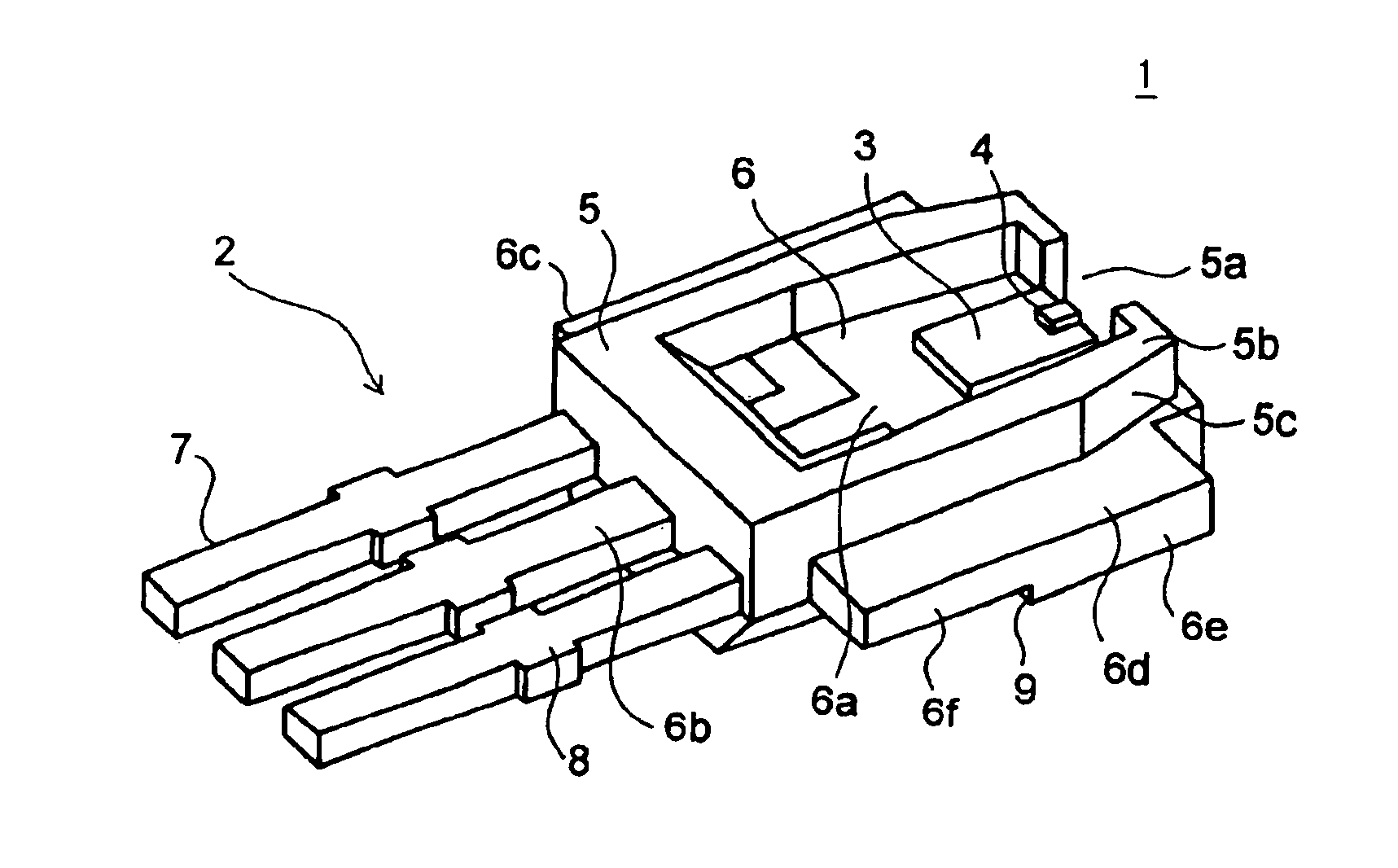
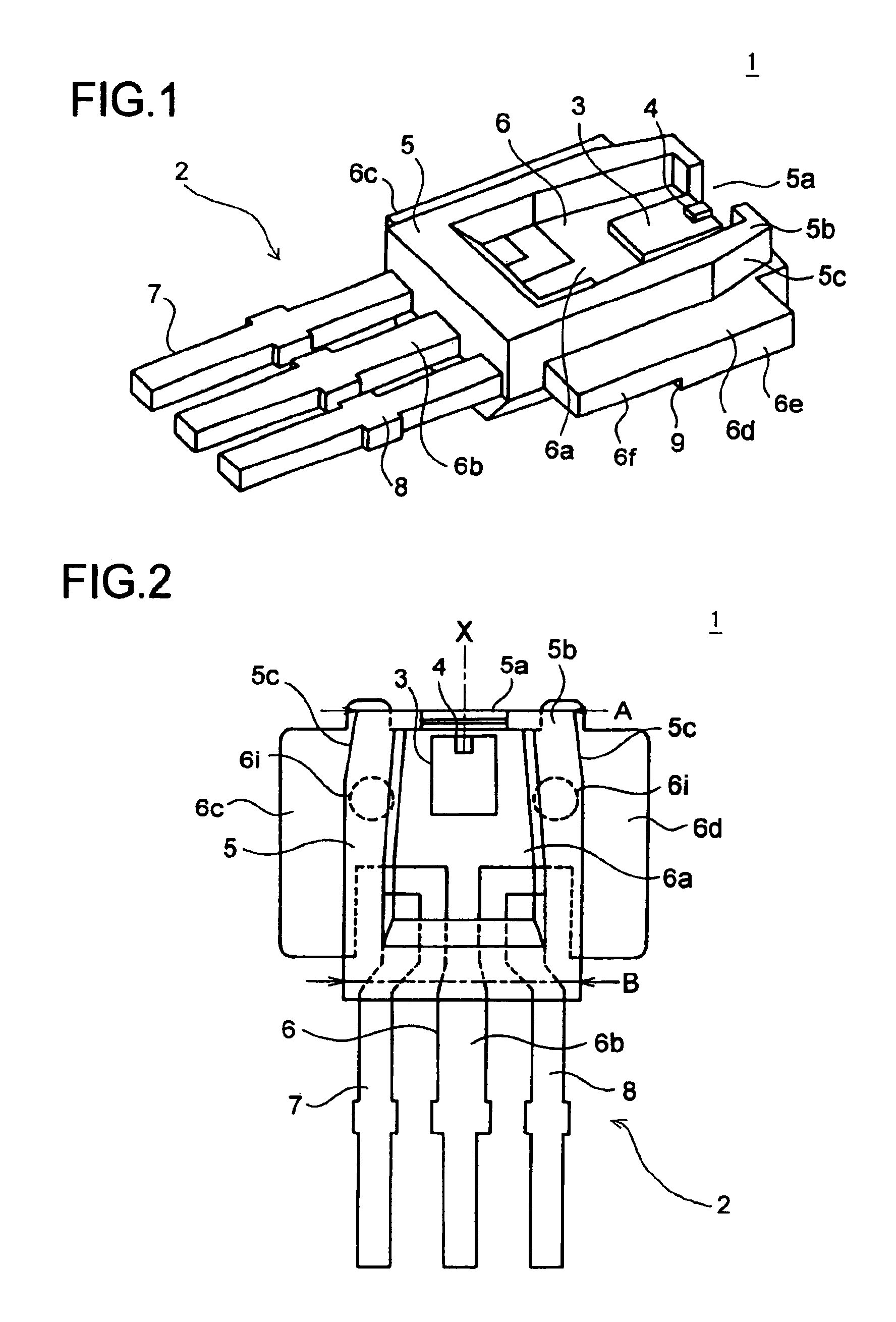
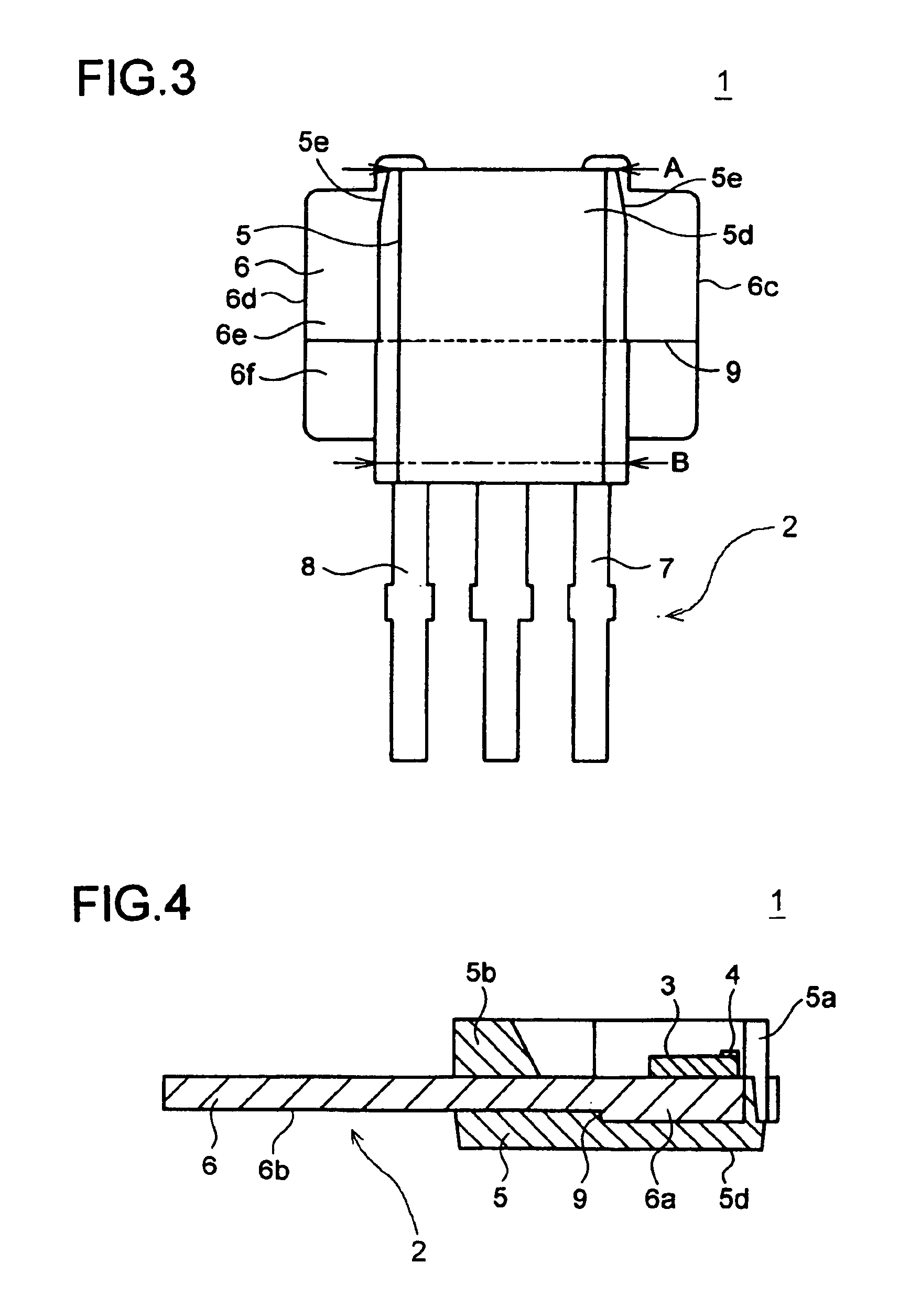
[0030]First, a first embodiment of the invention will be described with reference to the drawings. FIG. 1 is a perspective view of the semiconductor laser device of the first embodiment of the invention. FIG. 2 is a front view of the semiconductor laser device of the first embodiment of the invention. FIG. 3 is a rear view of the semiconductor laser device of the first embodiment of the invention. FIG. 4 is a sectional view of the semiconductor laser device of the first embodiment of the invention.

[0031]In the semiconductor laser device 1 of this embodiment, a submount 3 is disposed on and fixed to the top face of a lead frame 2, a semiconductor laser element 4 is disposed on and fixed to the top face of the submount 3, and the lead frame 2 is kept fixed by a resin 5 disposed in intimate contact therewith.

[0032]The lead frame 2 is made of a metal having high thermal and electrical conductivity, and is formed out of copper, iron, an alloy thereof, or the like into the shape of a plat...


PUM


Abstract

A semiconductor laser device includes a semiconductor laser element, a lead having an element disposing section where elements are disposed and a resin bonded to the lead. The lead has a thick portion and a thin portion with the thick portion being formed to extend at least in the direction of the width of the resin to cover a region having a length equal to or greater then the width of the resin. A semiconductor laser device has a semiconductor laser element, a lead having an element mount portion on which the semiconductor laser element is mounted and a resin maintained in intimate contact with the lead. The lead has a thicker portion and a thinner portion. The thicker portion is formed to extend in the direction of the width of the resin over a width equal to or greater than the width of the resin.

Description

TECHNICAL FIELD[0001]The present invention relates to a semiconductor laser device.BACKGROUND ART[0002]Much attention is paid to semiconductor laser devices employing a package composed of a lead frame and a resin molding, because they are comparatively inexpensive and easy to mass-produce. However, such resin molding packages suffer from poor heat rejection in comparison with metal can packages that have conventionally been widely used. For this reason, resin molding packages are now used almost exclusively in infrared lasers having good temperature characteristics, and not in high-output lasers for CD-R / W drives, or in infrared lasers for DVD drives, or in blue or similar lasers requiring high operating voltages. An improvement on a resin molding package for better heat dissipation is proposed, for example, in Japanese Patent Application Laid-Open No. H11-307871. According to this proposal, the portion of a lead on which a laser element is mounted is made thicker, and the lead is ...

Claims


Application Information

Patent Timeline
Patent Type & Authority Patents(United States)
IPC IPC(8): H01L23/495H01L23/48H01L33/00H01S5/00H01S5/022H01S5/02H01S5/024H01S5/026H01L33/62H01S5/0232
CPCH01L33/62H01S5/02244H01L2224/48247H01L2924/01039H01L2924/01079H01L2924/01021H01S5/02248H01S5/02469H01S5/0683H01S5/02325H01S5/0232
Inventor HONDA, SHOJIWATANABE, YASUHIROBESSHO, YASUYUKITANAKA, KENTAROU
Owner SANYO ELECTRIC CO LTD
Why Eureka
Try Eureka