Process to manufacture a top spin valve

a manufacturing process and spin valve technology, applied in the field of magnetic recording, can solve the problems of significant increase in the resistance of the entire structure, and the shield-to-shield separation of the spin valve head cannot be below about 800 , achieve the effect of narrowing the feedback pulse width and large shield-to-shield spacing

Inactive Publication Date: 2005-04-26
HEADWAY TECH INC
View PDF4 Cites 7 Cited by
  • Summary
  • Abstract
  • Description
  • Claims
  • Application Information

AI Technical Summary

Benefits of technology

[0010]It has been an object of the present invention to provide a spin valve structure that is free of internal electrical shorting by maintaining a relatively large shield-to-shield spacing while continuing to obtain very narrow feedback pulse widths.

Problems solved by technology

Furthermore, only the unaffected electrons will have mean free paths long enough for them to have a high probability of crossing the non magnetic layer.
However, once these electrons ‘switch sides’, they are immediately subject to increased scattering, thereby becoming unlikely to return to their original side, the overall result being a significant increase in the resistance of the entire structure.
Currently, the shield-to-shield separation of a spin valve head cannot be below about 800 Å, mainly due to the sensor-to-shield shorting problem.

Method used


Image

  • Process to manufacture a top spin valve
  • Process to manufacture a top spin valve
  • Process to manufacture a top spin valve

Examples


first embodiment

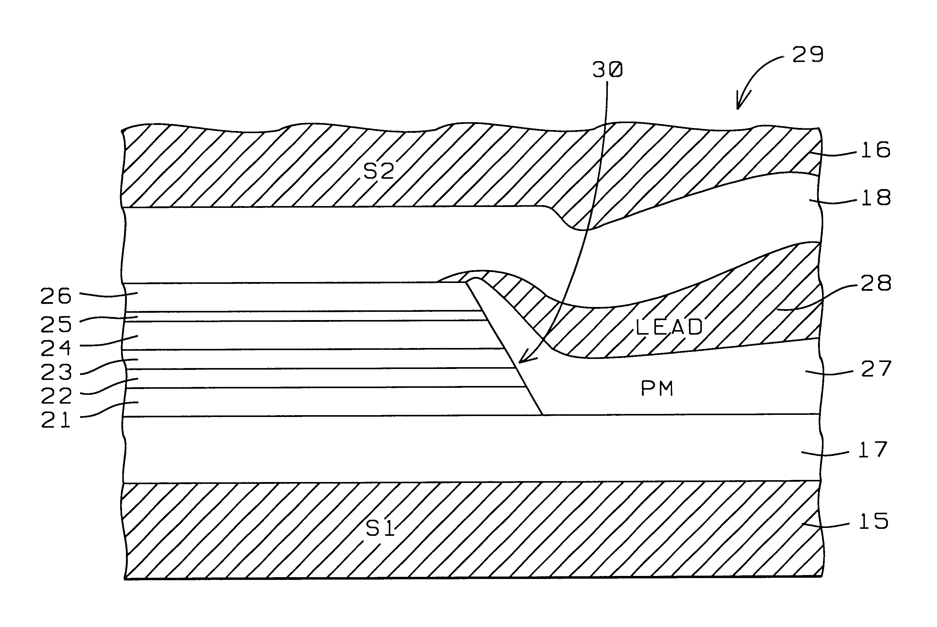
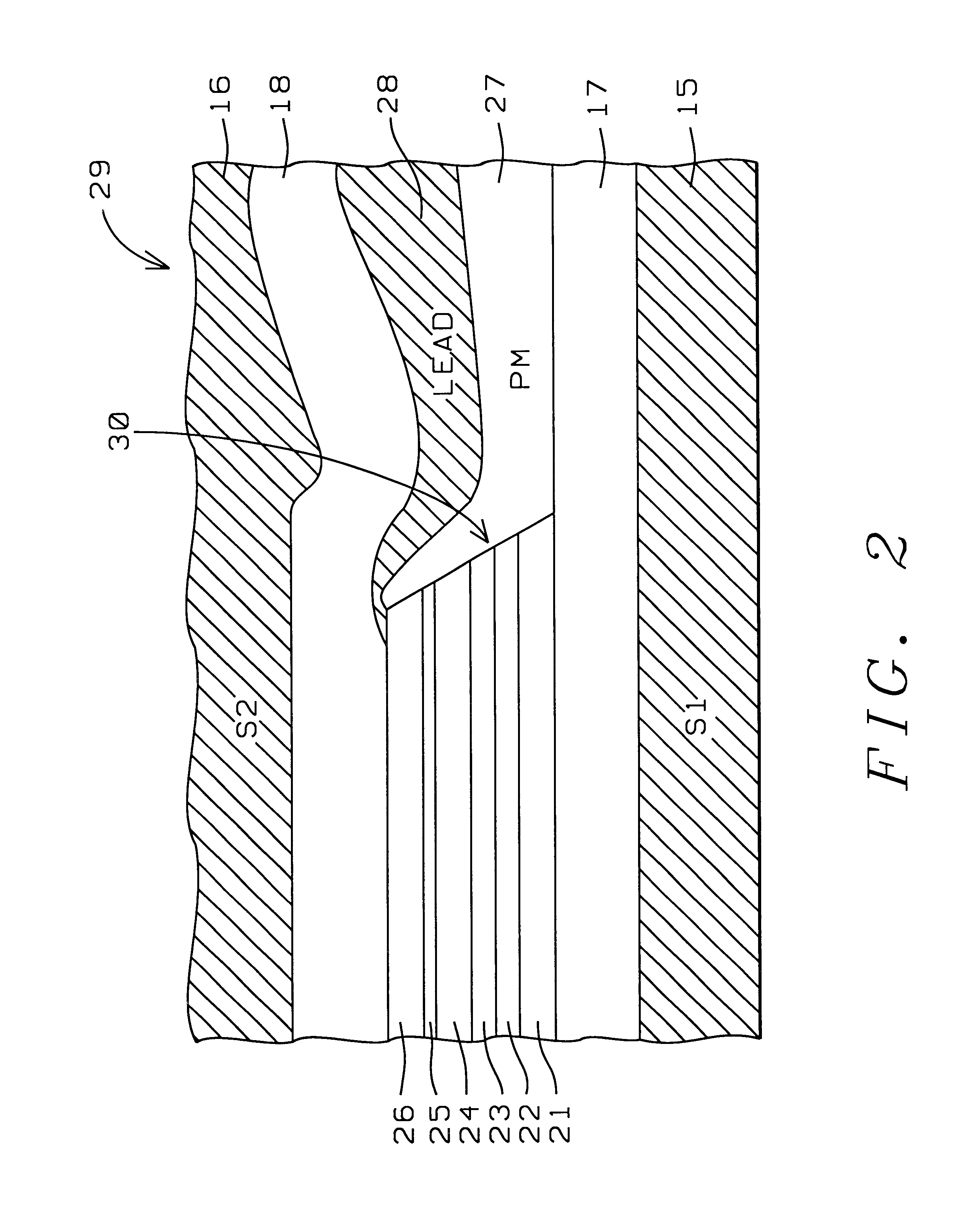
[0025]This process is for manufacturing a top spin valve structure. It begins with the provision the first (lower) of the two primary magnetic shields. This can be seen as layer 15 in FIG. 2 on which dielectric layer 17 is deposited, followed by the deposition of free layer 21. This is followed by the deposition of non-magnetic layer 22 onto which is deposited pinned layer 23. Next, onto pinned layer 23 there is deposited anti-ferromagnetic layer 24 for use as a pinning layer. This completes formation of the spin valve itself.

[0026]Now follows a key feature of the invention. On anti-ferromagnetic layer 24, decoupling layer 25 is deposited, followed by the deposition of thin film shield 26. The purpose of the decoupling layer is to avoid any exchange coupling of the thin film shield by layer 24. The thin film shield is a layer of ferromagnetic material having a permeability greater than about 500. It needs to have as high an electrical resistivity as possible within other constraints...

second embodiment

[0029]This process is also for manufacturing a top spin valve structure. Referring now to FIG. 3, this embodiment begins with the provision of the first (lower) of the two primary magnetic shields 15 on which dielectric layer 17 is deposited. Now follows a key feature of the invention, namely the deposition of thin film shield 36. The thin film shield is a layer of high permeability (greater than about 500) ferromagnetic material. It needs to have as high an electrical resistivity as possible within other constraints of the structure. It is required to be at least 5 times more resistive than the free layer. Since the latter is about 25 micro-ohm-cm, a value greater than about 125 micro-ohm-cm is to be preferred. The thickness of the thin film shield should be such that the moment-thickness product (of the thin film shield) is 2-5 times that of the free layer. The presence of this thin film shield allows relatively thicker dielectric layers to be used, thereby reducing or eliminating...

third embodiment

[0033]This process is also for manufacturing a top spin valve structure. We refer now to FIG. 4 which begins with the provision of the first (lower) of the two primary magnetic shields 15 onto which is deposited dielectric layer 17. Then, on a selected area at the surface of layer 17, a layer of conductive material 47, suitable for use as a connecting lead to the structure, is deposited. Then, on layer 47 only, layer 48 of a ferromagnetic material suitable for use as an exchange magnet is deposited. This will serve to provide the needed longitudinal bias for the structure, as discussed above.

[0034]Then, free layer 21 is deposited over the full surface followed by the deposition of non-magnetic layer 22 onto which is deposited pinned layer 23. Next, onto pinned layer 23 there is deposited anti-ferromagnetic layer 24 for use as a pinning layer.

[0035]Now follows a key feature of the invention. On anti-ferromagnetic layer 24, decoupling layer 25 is deposited, followed by the deposition ...


PUM

PropertyMeasurementUnit
angleaaaaaaaaaa
magneticaaaaaaaaaa
non-magnetic aaaaaaaaaa

Abstract

Currently, the shield-to-shield separation of a spin valve head cannot be below about 800 Å, mainly due to sensor-to-lead shorting problems. This problem has now been overcome by inserting a high permeability, high resistivity, thin film shield on the top or bottom (or both) sides of the spin valve sensor. A permeability greater than about 500 is required together with a resistivity about 5 times greater than that of the free layer and an MrT value for the thin film shield that is 4 times greater than that of the free layer. Five embodiments of the invention are described.

Description

FIELD OF THE INVENTION[0001]The invention relates to the general field of magnetic recording with particular reference to improving linear resolution.BACKGROUND OF THE INVENTION[0002]The present invention is concerned with the manufacture of the read element in a magnetic disk system. This is a thin slice of material located between two magnetic shields which we will refer to a primary shields. The principle governing operation of the read sensor is the change of resistivity of certain materials in the presence of a magnetic field (magneto-resistance). In particular, most magnetic materials exhibit anisotropic behavior in that they have a preferred direction along which they are most easily magnetized (known as the easy axis). The magneto-resistance effect manifests itself as a decrease in resistivity when the material is magnetized in a direction perpendicular to the easy axis, said decrease being reduced to zero when magnetization is along the easy axis. Thus, any magnetic field t...

Claims


Application Information

Patent Timeline
Patent Type & Authority Patents(United States)
IPC IPC(8): B05D7/00G01R33/06G01R33/09G11B5/127G11B5/187H01F10/00H01F10/30G11B5/33G11B5/39H01F10/12H01F10/32H01L43/00H01F10/16H01L43/08H01L43/12H04R31/00G11B5/29G11B5/31
CPCG11B5/29G11B5/31G11B5/33Y10T29/49046Y10T29/49037Y10T29/49043Y10T29/49044Y10T29/49041Y10T29/49052
Inventor JU, KOCHANHORNG, CHENGZHENG, YOUFENGLIAO, SIMONCHANG, JEI-WEI
Owner HEADWAY TECH INC
Why Eureka
Try Eureka