

STI stress modification by nitrogen plasma treatment for improving performance in small width devices
a technology of nitrogen plasma treatment and stress modification, which is applied in the field of semiconductor processing, can solve the problems of negative impact on some devices, positive impact on other devices, device improvement, etc., and achieve the effect of increasing the device performance of the p
- Summary
- Abstract
- Description
- Claims
- Application Information
AI Technical Summary
Benefits of technology
Problems solved by technology
Method used
Image

Examples
Embodiment Construction
[0039]The present invention, which provides a method for modifying the stress caused by bird beak formation in the isolation regions of small width CMOS devices, will now be described in greater detail by referring to the drawings that accompany the present application. In the drawings representing the present invention, like reference numerals are used in describing like and / or corresponding elements.
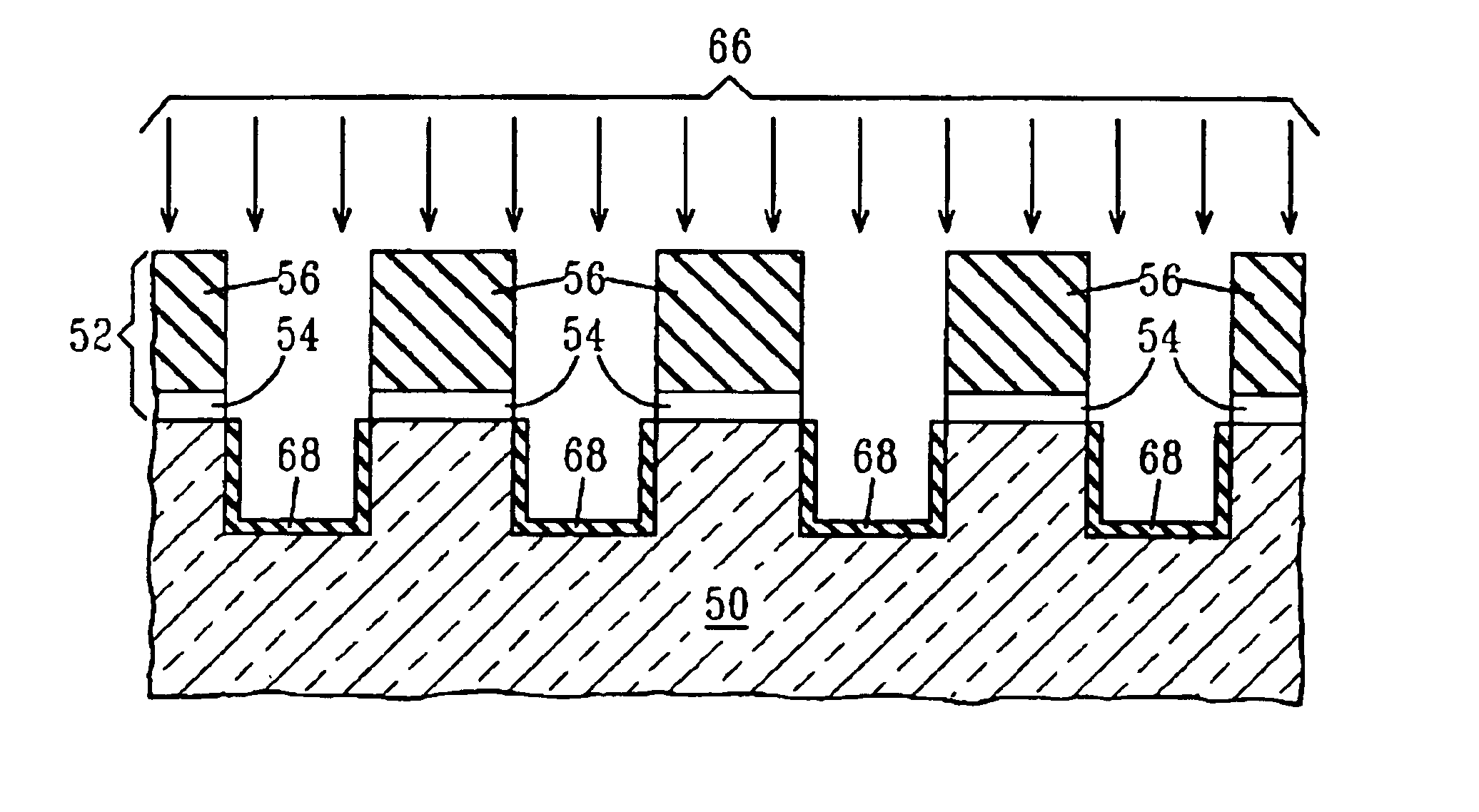
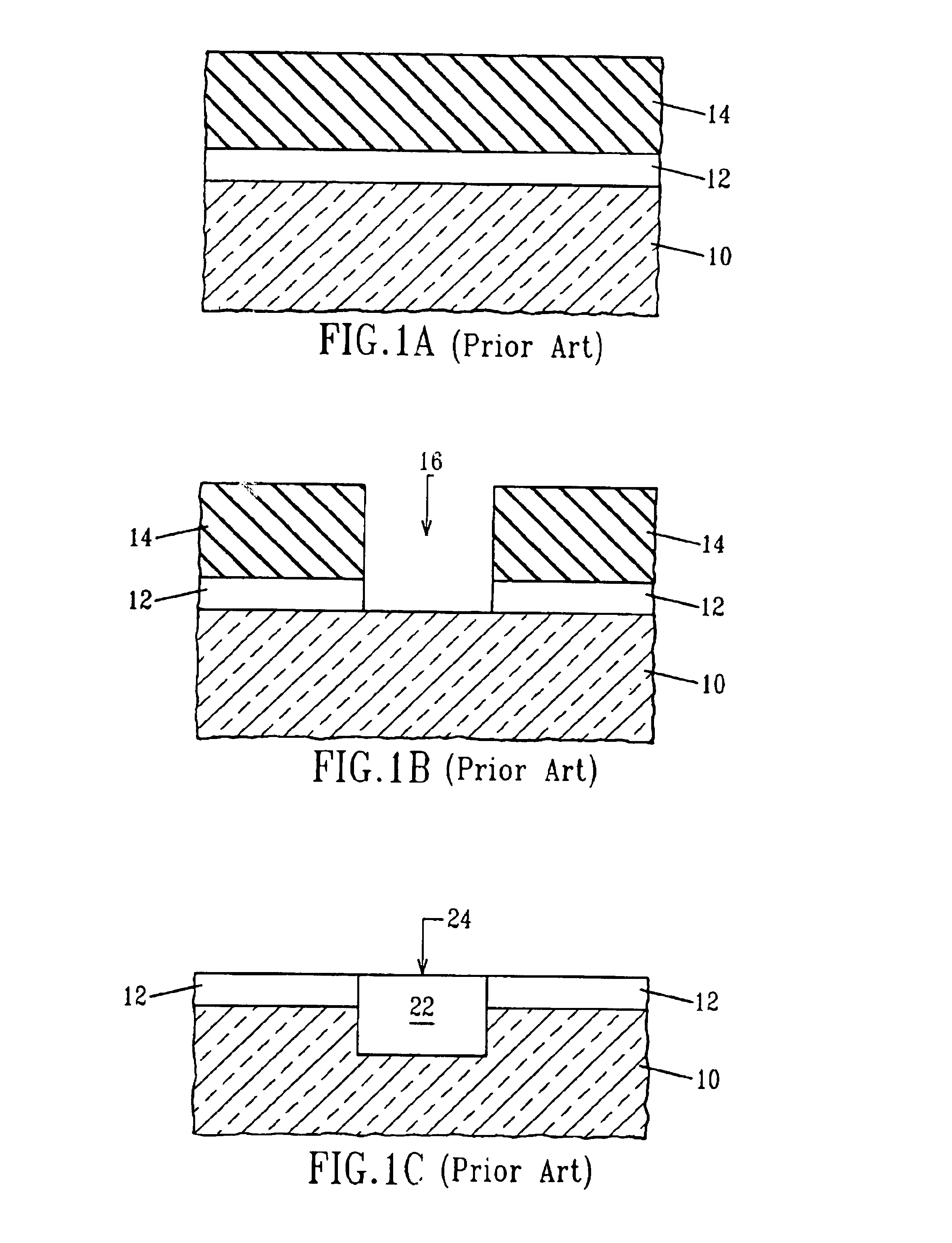
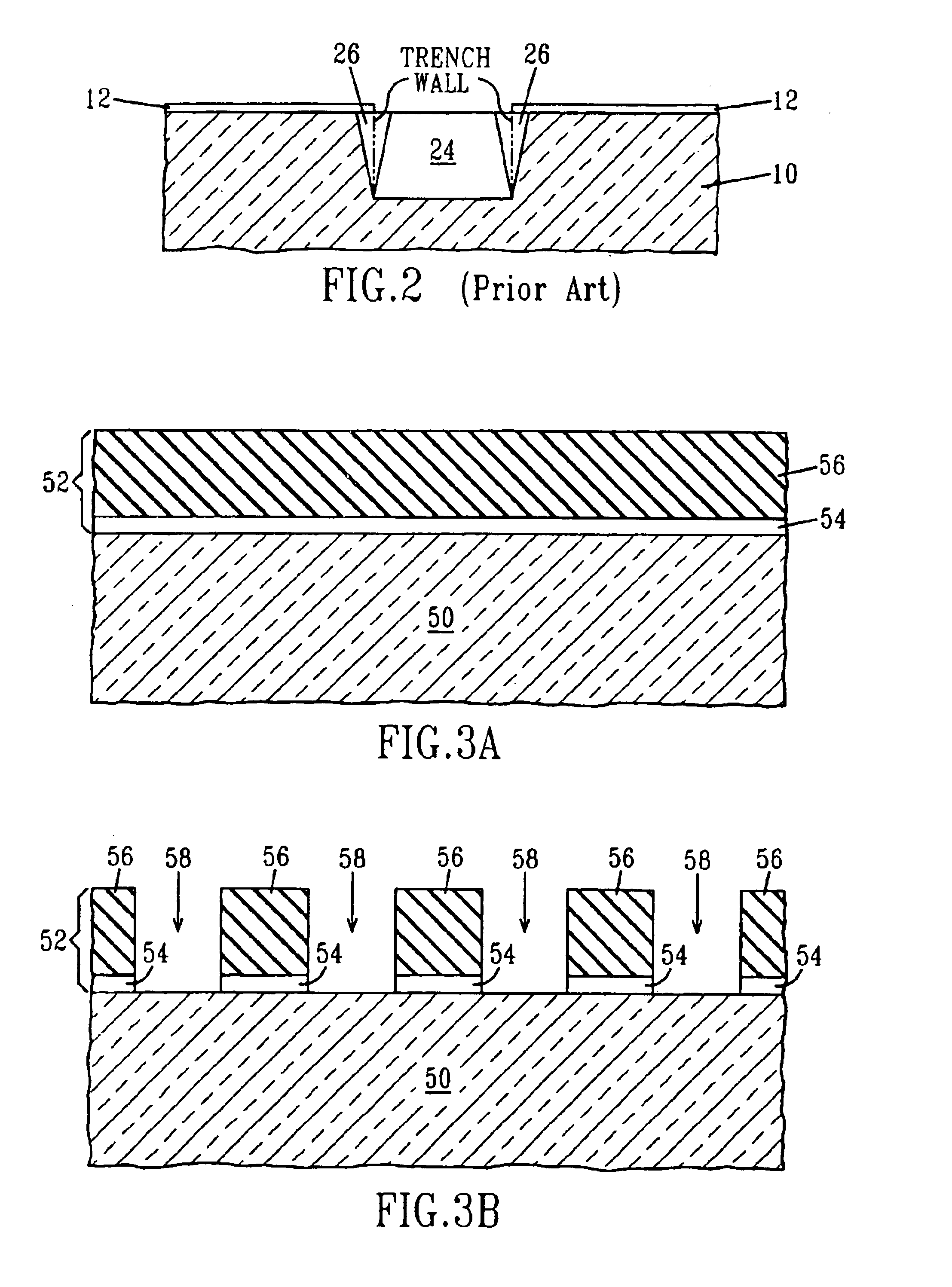
[0040]Reference is first made to the embodiment depicted in FIGS. 3A-3E. 3E. In this embodiment of the present invention, the trench is subjected to a plasma nitridation process prior to filling the trench with a trench fill material. Specifically, FIG. 3A shows an initial structure of the first embodiment of the present application. In FIG. 3A, there is shown a semiconductor substrate 50 having a material stack 52 located on a surface of the semiconductor substrate 50. Material stack 52 comprises at least a pad oxide 54 and a pad nitride 56. As shown, the pad oxide 54 is located on an...
PUM
 Abstract
Description
Claims
Application Information