Indium oxide conductive film
- Summary
- Abstract
- Description
- Claims
- Application Information
AI Technical Summary
Benefits of technology
Problems solved by technology
Method used
Image
Examples
Embodiment Construction
[0031]OF THE PREFERRED EMBODIMENTS
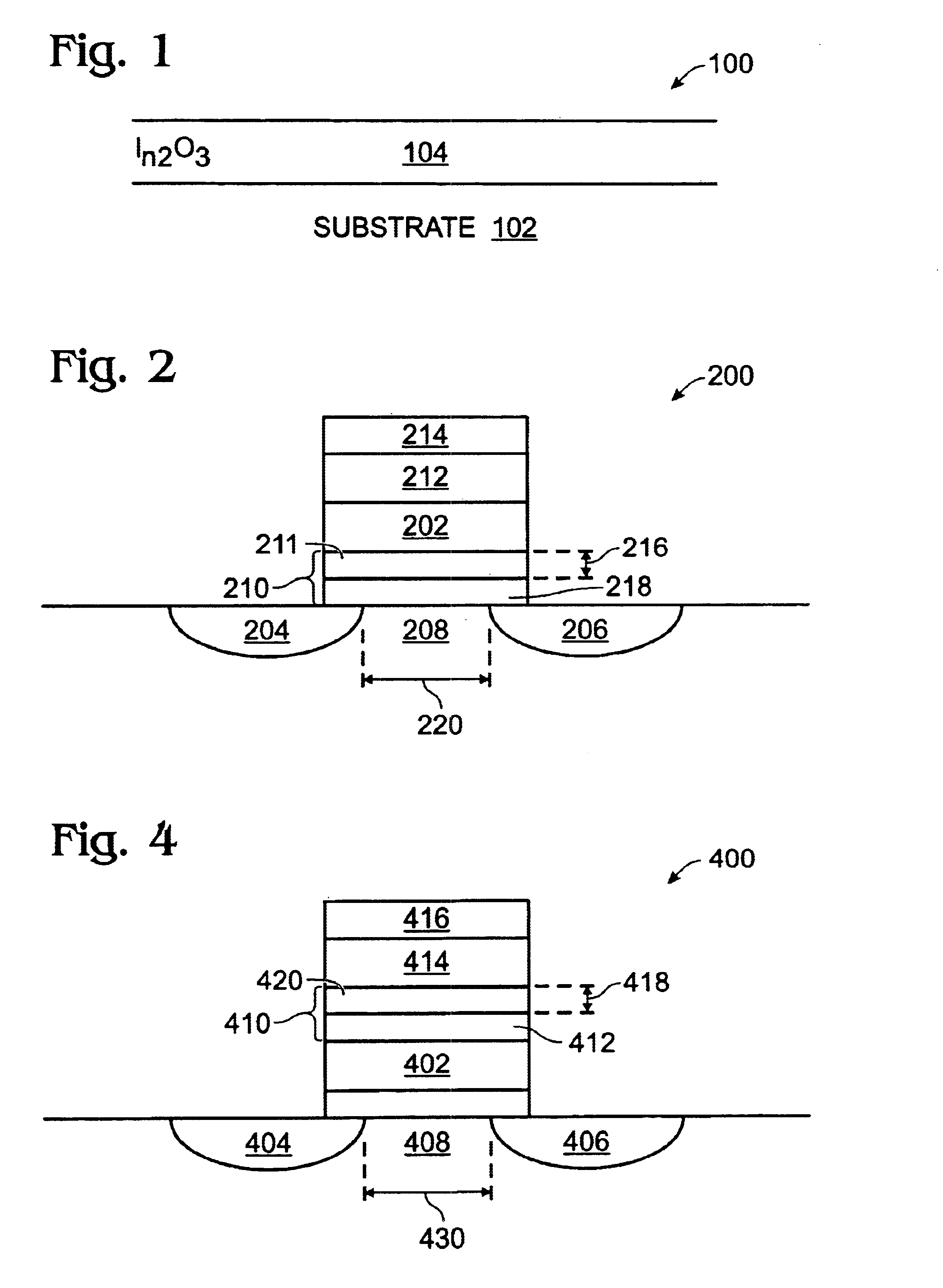
[0032]FIG. 1 is a partial cross-sectional view of the present invention indium oxide (In2O3) film structure. The film structure 100 comprises a substrate 102 and an In2O3 film 104 overlying the substrate 102, having a resistivity in the range of 260 to 800 ohm-cm. The substrate 102 can be a material such as platinum (Pt), iridium (Ir), other noble metals, silicon (Si), high-k oxides, or silicon dioxide (SiO2).
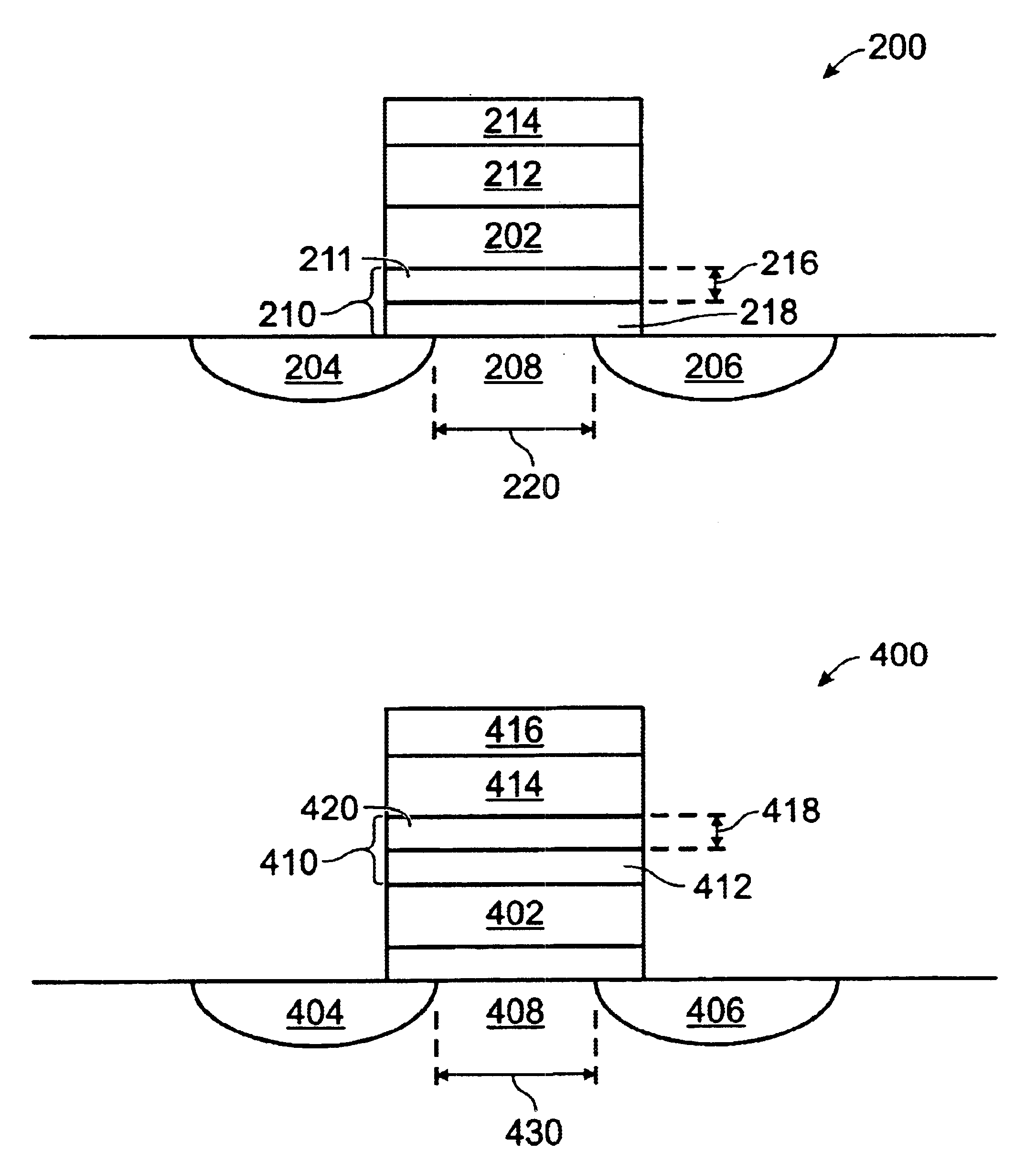
[0033]FIG. 2 is a partial cross-sectional view of the present invention 1T memory device using an In2O3 film as a gate insulator. The device 200 comprises a CMOS transistor gate 202, source 204, drain 206, and channel region 208. A gate insulator 210 is formed from an In2O3 thin film 211, interposed between the channel region 208 and the gate 202. The In2O3 film 211 has a resistivity in the range of 260 to 800 ohm-cm. A memory cell film 212 overlies the gate electrode 202. A top electrode 214 overlies the memory cell film 212.
[0034]The In2O3 th...
PUM
 Abstract
Description
Claims
Application Information


