Integrated circuit and method for testing same using single pin to control test mode and normal mode operation

a technology of integrated circuits and single pins, applied in logic circuit coupling/interface arrangements, pulse techniques, instruments, etc., can solve the problems of increasing the cost of electronic systems, requiring high investment, and traditional trimming techniques that are expensive to implement. achieve the effect of reducing power consumption

Inactive Publication Date: 2005-05-03
NAT SEMICON CORP
View PDF6 Cites 27 Cited by
  • Summary
  • Abstract
  • Description
  • Claims
  • Application Information

AI Technical Summary

Benefits of technology

[0014]In preferred embodiments, when the test circuitry is neither in the test mode nor in a receptive mode in which it analyzes test data b

Problems solved by technology

However, prior art trimming techniques are traditionally very exp

Method used


Image

  • Integrated circuit and method for testing same using single pin to control test mode and normal mode operation
  • Integrated circuit and method for testing same using single pin to control test mode and normal mode operation
  • Integrated circuit and method for testing same using single pin to control test mode and normal mode operation

Examples


Embodiment Construction

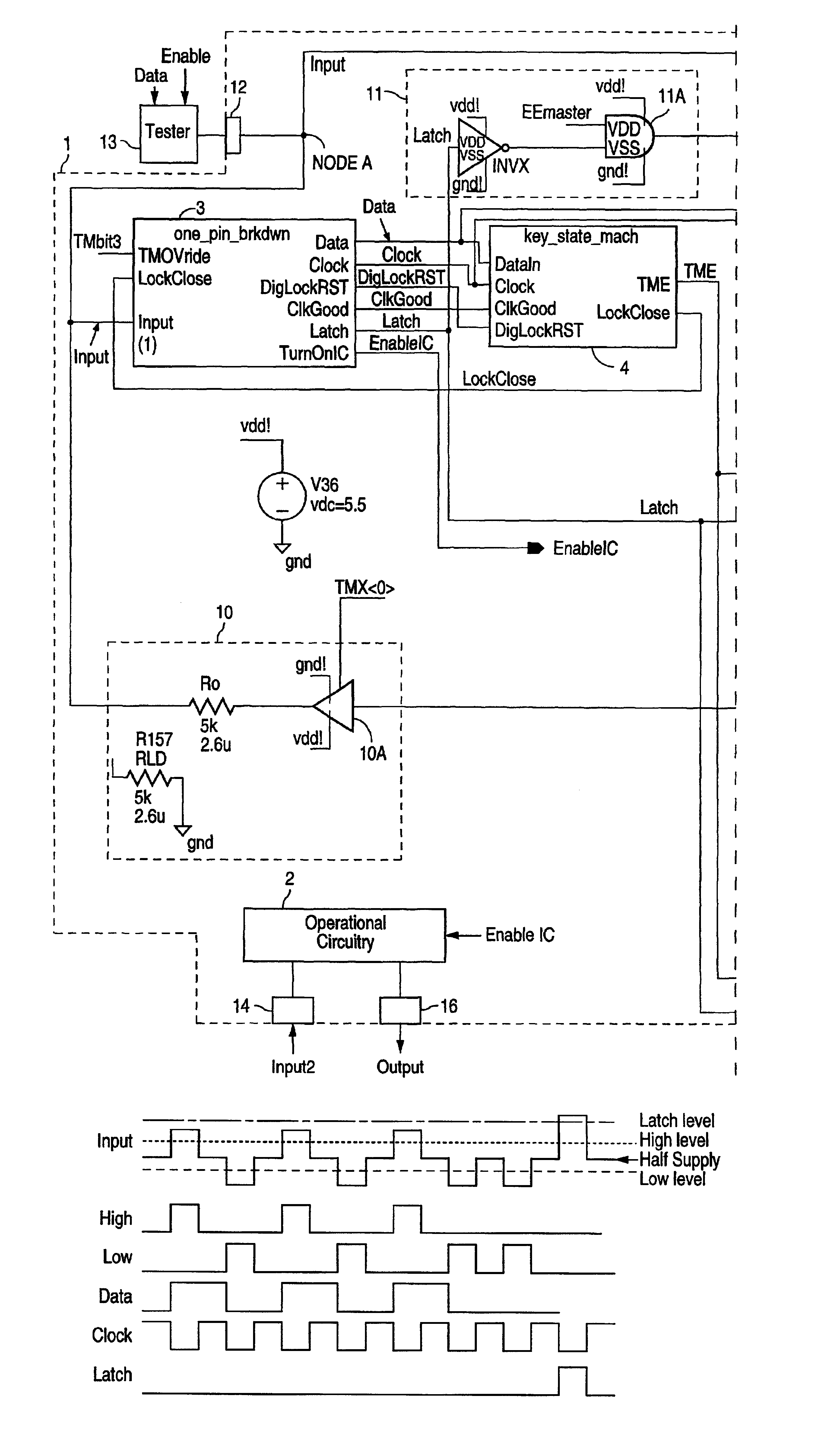
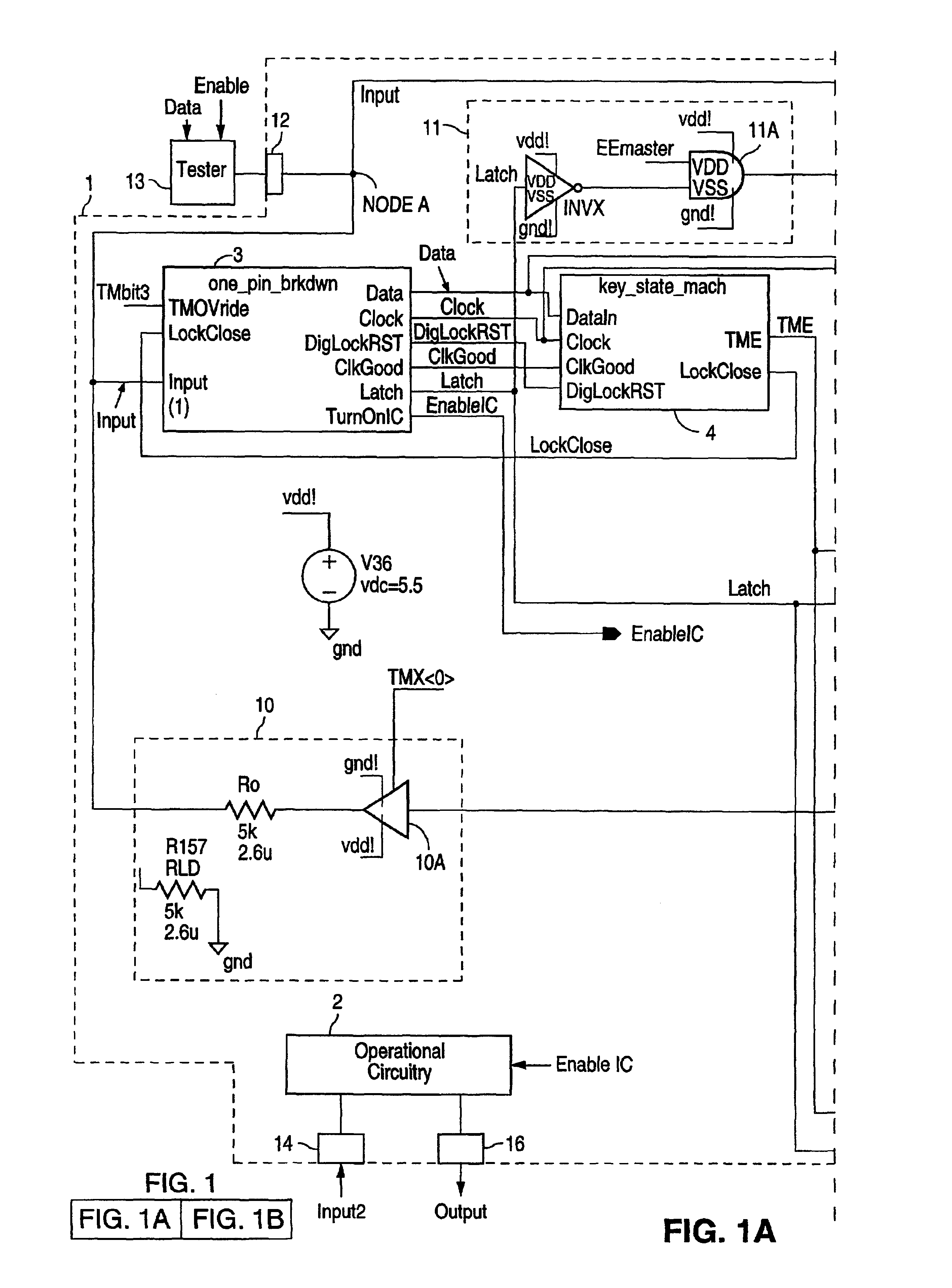
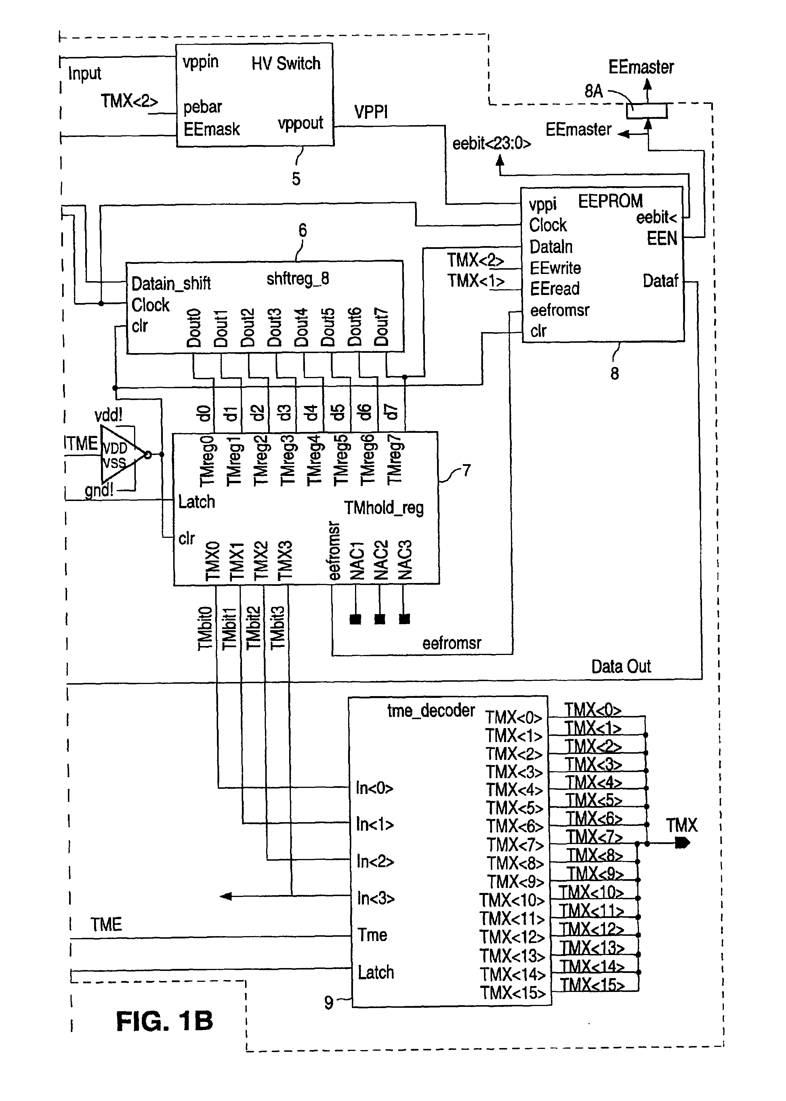
[0028]A preferred embodiment of the invention will be described with reference to FIGS. 1 and 6-13. Signals generated during operation of this embodiment of the invention will be discussed with reference to FIGS. 2-5.

[0029]Integrated circuit 1 (“chip”1) of FIG. 1 includes operational circuitry 2, and test mode circuitry comprising input logic 3, state machine 4, high voltage switch 5, shift register circuitry 6, register 7, EEPROM 8, decoder 9, and output buffer circuitry 10, connected as shown in FIG. 1. Pad 12 of chip 1 (at Node A, an external node of chip 1) is connected to external test circuit 13 (e.g., by a wire between pad 12 and circuit 13) during operation of chip 1. Circuit 13 asserts a modulated Enable signal (labeled “Input”) to pad 12, and receives output test data (from EEPROM 8, and labeled “Data Out” in FIG. 1) that is asserted via buffer circuitry 10 to pad 12. Operational circuitry 2 can include digital circuitry, analog circuitry or both. In a normal operating mod...


PUM


Abstract

An integrated circuit including operational circuitry operable in response to at least one control signal asserted to an external node from an external source, and test circuitry coupled to the external node and the operational circuitry. In response to data asserted to the external node from an external source, the test circuitry enters a test mode in which it tests, configures, or reconfigures the operational circuitry. The test circuitry also asserts to the operational circuitry each control signal received at the external node (or an amplified or translated version thereof). Other aspects of the invention include test circuitry for use in a circuit having an access node and methods for performing on-chip testing, configuration, and control of operational circuitry within a chip in response to test data and at least one control signal asserted from an external source to an external node.

Description

BACKGROUND OF THE INVENTION[0001]1. Field of the Invention[0002]The present invention relates to integrated circuits including test mode circuitry and methods for testing such integrated circuits. More specifically, the inventive method is a method for testing an integrated circuit (“chip”) in which test data are sent to or from (or both to and from) the chip via one pin, the pin is also used in a normal operating mode to assert at least one signal to or from the chip, and the pin is optionally also used in a third mode (or in the test mode) for sending signals to circuitry of the chip for trimming or reconfiguring the chip.[0003]2. Description of the Related Art[0004]The quest to produce integrated circuits that operate with higher accuracy has led to a need for testing and final adjustment (e.g., at the manufacturing facility) of the performance of manufactured chips. Various methods have been used to improve performance of chips after they have been manufactured, including variou...

Claims


Application Information

Patent Timeline
IPC IPC(8): G06F13/00H03K19/0175G01R31/317
CPCG01R31/31713G01R31/31701
Inventor KOTOWSKI, JEFFREY P.FODCHUK, KYLE
Owner NAT SEMICON CORP
Why Eureka
Try Eureka