Method for fabricating a P-N heterojunction device utilizing HVPE grown III-V compound layers and resultant device
Inactive Publication Date: 2005-05-10
KYMA TECH
View PDF55 Cites 36 Cited by
Summary
Abstract
Description
Claims
Application Information
AI Technical Summary
This helps you quickly interpret patents by identifying the three key elements:
Problems solved by technology
Method used
Benefits of technology
[0010]The present invention provides a method for fabricating p-n heterojunction devices using HVPE techniques. If desired, t
Problems solved by technology
In particular, these materials exhibit a direct band gap structure, high electric field breakdown, and high thermal conductivity.
Unfortunately, although the III-V compounds are attractive for semiconductor applications due to their physical and electronic properties, until recently the development of devices based on III-V compounds has been limited by the lack of material with suitable conductivity, specifically p-type material.
Although the MOCVD technique has proven adequate for a variety of commercial devices, it has a number of limitations that constrain the useful
Method used
Image
Click on the blue label to locate the original text in one second.
Reading with bidirectional positioning of images and text.
Examples
Embodiment Construction
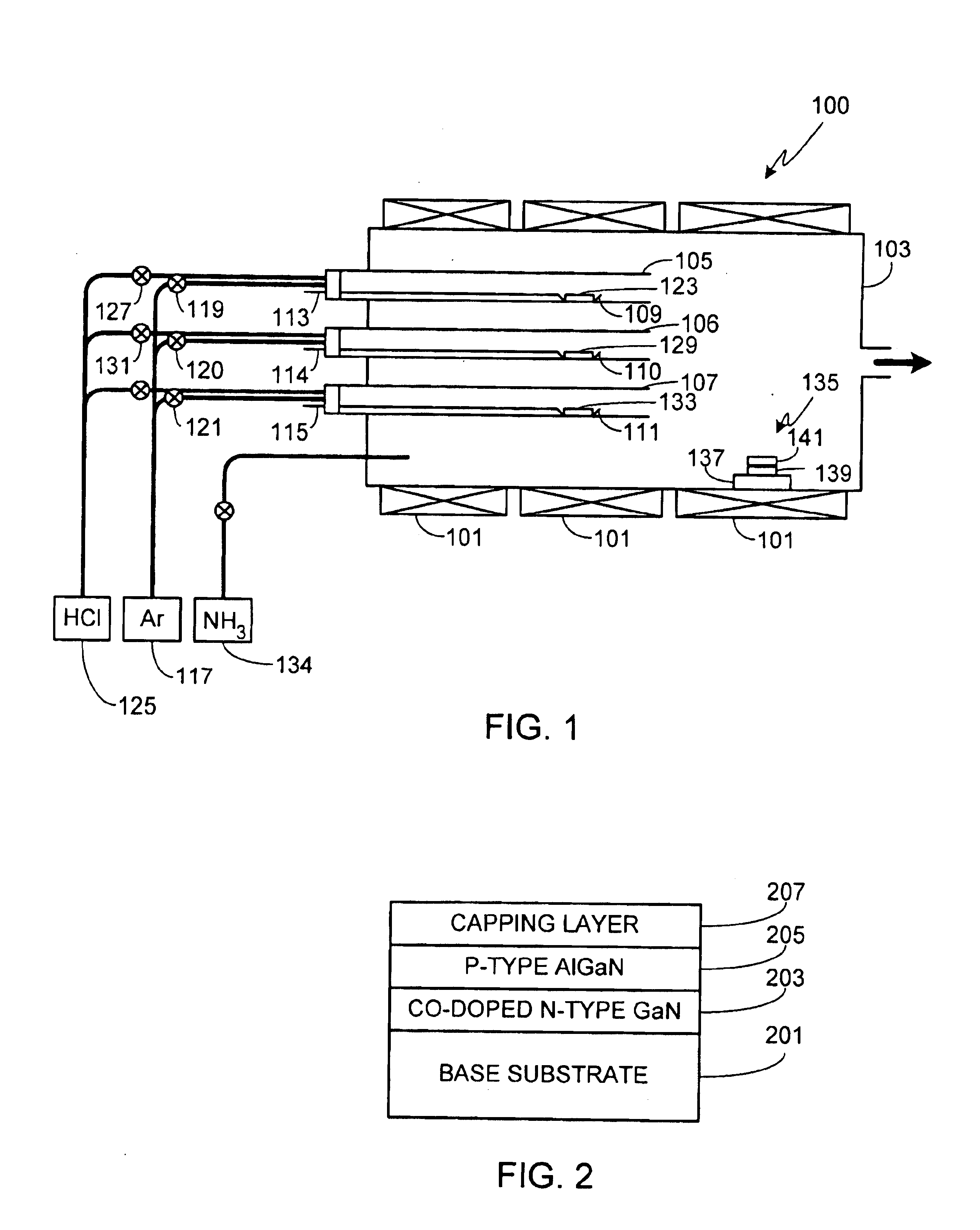
[0017]FIG. 1 is a schematic illustration of a horizontal furnace as used with the invention. It should be understood that the invention is not limited to this particular furnace configuration as other furnace configurations (e.g., vertical furnaces) that offer the required control over the temperature, temperature zones, gas flow, source location, substrate location, etc., can also be used. Furnace 100 is comprised of multiple temperature zones, preferably obtained by using multiple heaters 101, each of which at least partially surrounds furnace tube 103. Within furnace tube 103 are multiple source tubes 105-107. It will be understood that additional source tubes may be used in furnace 100, depending upon the desired composition of the required layers. Although source tubes are used in the preferred embodiment of the invention, other means of separating the sources can be used, such as furnace partitions. Preferably source tubes 105-107 are comprised of quartz.
[0018]Within each sour...
PUM
Abstract
A method for fabricating a p-n heterojunction device is provided, the device being preferably comprised of an n-type GaN layer co-doped with silicon and zinc and a p-type AlGaN layer. The device may also include a p-type GaN capping layer. The device can be grown on any of a variety of different base substrates, the base substrate comprised of either a single substrate or a single substrate and an intermediary layer. The device can be grown directly onto the surface of the substrate without the inclusion of a low temperature buffer layer.
Description
CROSS-REFERENCES TO RELATED APPLICATIONS[0001]This application is a continuation-in-part application of U.S. patent application Ser. No. 09 / 860,651, filed May 18, 2001 now U.S. Pat. No. 6,559,038, which is a continuation-in-part application of U.S. patent application Ser. No. 09 / 638,638, filed Aug. 14, 2000 now abandoned, which is a divisional of U.S. patent application Ser. No. 09 / 195,217 filed Nov. 18, 1998 now U.S. Pat. No. 6,218,269, which claims the benefit of U.S. patent application Ser. No. 60 / 066,940 filed Nov. 18, 1997, the disclosures of which are incorporated herein by reference for all purposes.FIELD OF THE INVENTION[0002]The present invention relates generally to semiconductor devices and, more particularly, to a method for fabricating p-n heterojunction-based devices utilizing III-V compound layers as well as the structures that result from the application of the method.BACKGROUND OF THE INVENTION[0003]III-v compounds such as GaN, AlN, AlGaN, and InAlGaN have unique ph...
Claims
Application Information
Patent Timeline
Application Date:The date an application was filed.
Publication Date:The date a patent or application was officially published.
First Publication Date:The earliest publication date of a patent with the same application number.
Issue Date:Publication date of the patent grant document.
PCT Entry Date:The Entry date of PCT National Phase.
Estimated Expiry Date:The statutory expiry date of a patent right according to the Patent Law, and it is the longest term of protection that the patent right can achieve without the termination of the patent right due to other reasons(Term extension factor has been taken into account ).
Invalid Date:Actual expiry date is based on effective date or publication date of legal transaction data of invalid patent.