Electronic device having controllable conductance

a technology of electronic devices and conductances, applied in the field of electronic elements, can solve the problems of difficult to manufacture electronic elements with such a function in practice, unsuitable inclusion methods in high density integrated circuits, and difficulty in incorporating such electric elements into circuits to make the electrode mov

Inactive Publication Date: 2005-05-10
JAPAN SCI & TECH CORP +1
View PDF2 Cites 5 Cited by
  • Summary
  • Abstract
  • Description
  • Claims
  • Application Information

AI Technical Summary

Problems solved by technology

However, in order to construct an electronic element using this technique, a piezo-electric element which can move an electrode (i.e., metal needle) is required, but it is difficult to incorporate such an electric element into a circuit to make the electrode move.
Further, as another electrode is required to drive the piezo-electric element, the method is unsuitable for inclusion in a high density integrated circuit.
Thus, it is difficult to manufacture an electronic element with such a function in practice.

Method used


Image

  • Electronic device having controllable conductance
  • Electronic device having controllable conductance
  • Electronic device having controllable conductance

Examples


example 1

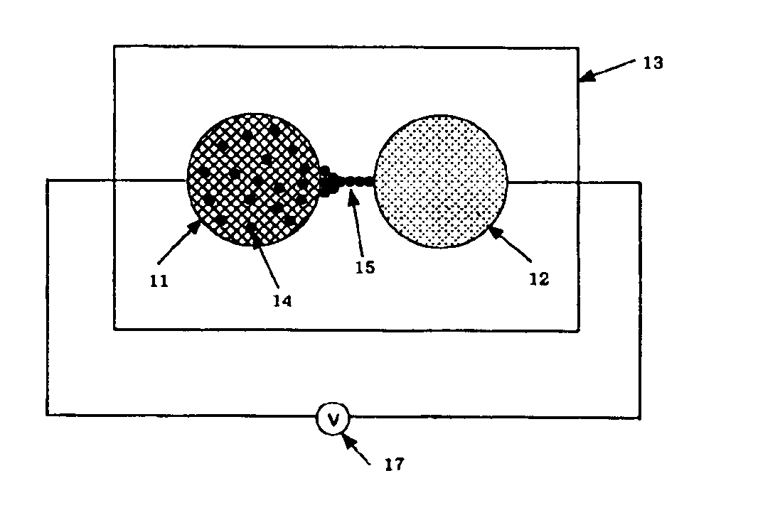
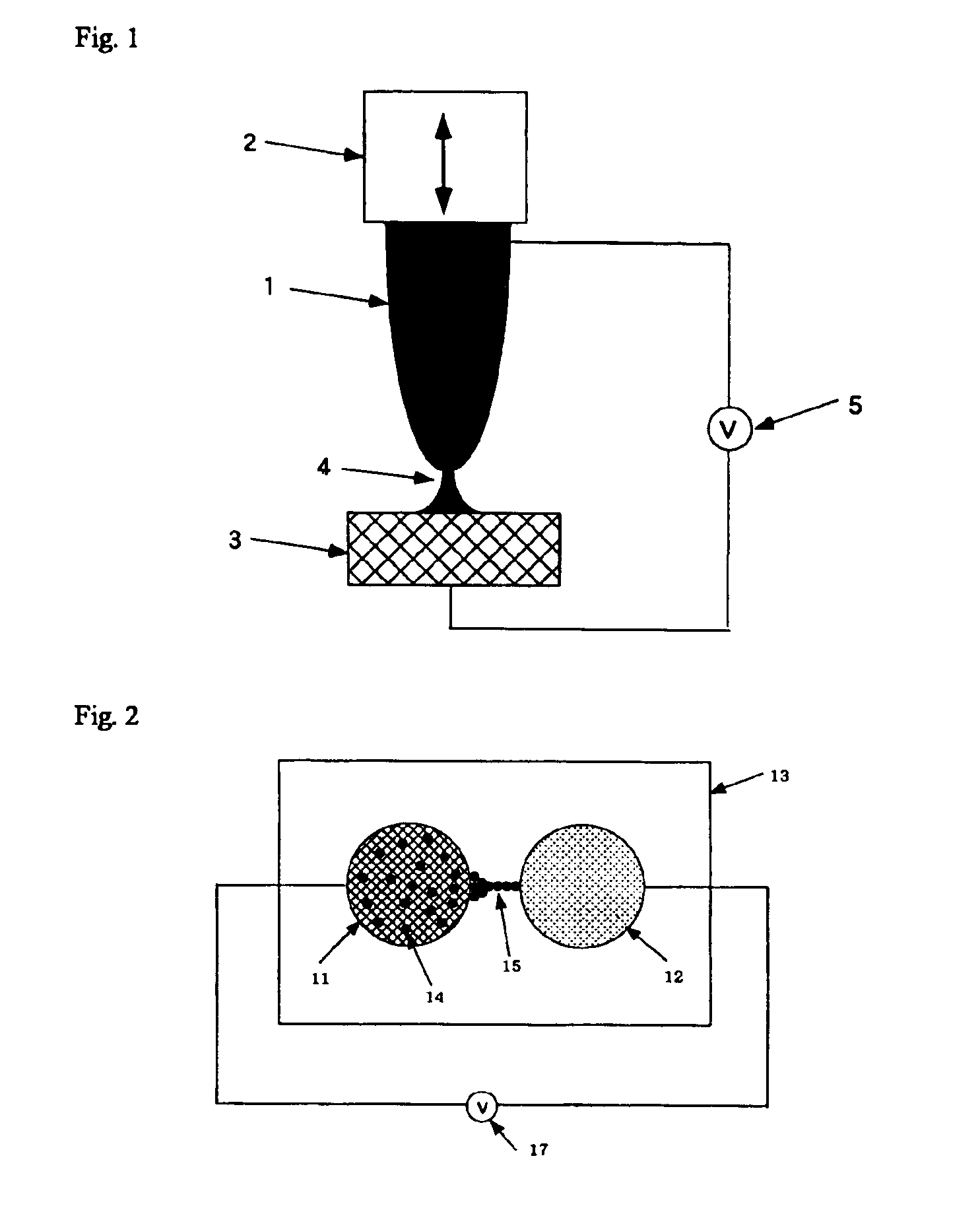
[0040]An electrode of a mixed electroconductor Ag2S crystal was first produced by vapor phase epitaxy. In this example, the material of the facing conductive electrode was platinum, and the substrate was an insulating material. The interval between these electrodes was about 1 nanometer, and a tunnel current was made to flow between the electrodes.

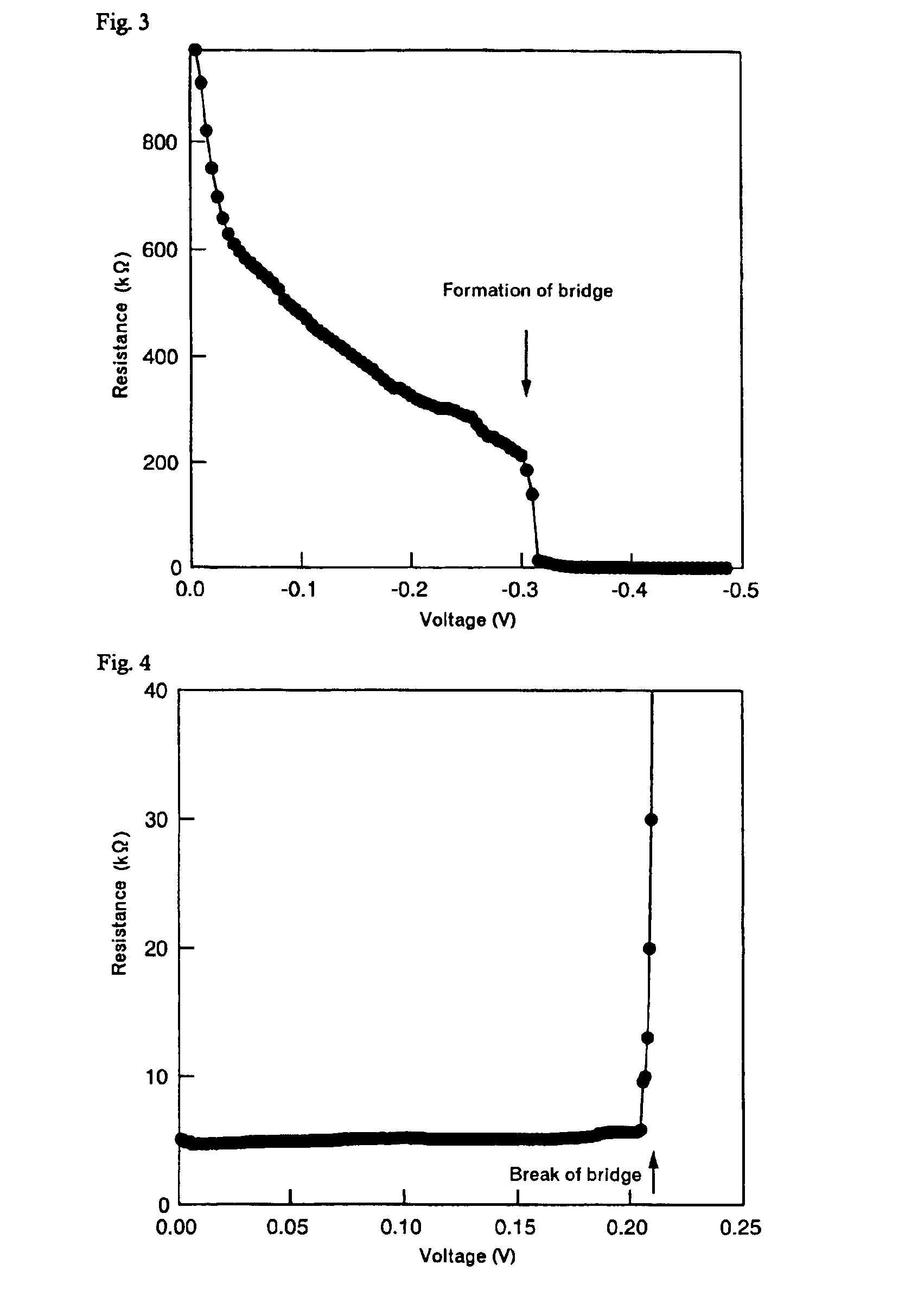
[0041]Using an electronic element manufactured in this way, a voltage was applied between the Ag2S electrode and the platinum electrode, and the voltage was swept at 50 mV / sec. The formation of a bridge between the electrodes is shown in FIG. 3. The voltage in the diagram shows the potential of the electroconducting electrode relative to the Ag2S electrode, based on the Ag2S electrode. When the applied volage is in the vicinity of V=0˜−0.3V, the inter-electrode resistance has a comparatively large value, and the resistance falls gradually as the voltage increases. This is due to the fact that movable silver ions (atoms) in the Ag2S electro...

example 2

[0042]FIG. 4 shows the case where, using an identical electronic element to that of Example 1, a bridge is disconnected. Herein, the polarity of the voltage applied was reversed from that used when the bridge was constructed. The resistance of the bridge increases slowly up to the vicinity of V=0˜0.20V. This is because the silver atoms forming the bridge gradually move and return to the Ag2S electrode, so the bridge gradually becomes thinner. A rapid increase in resistance is observed in the vicinity of V=0.20V. This rapid increase of resistance is due to the disconnection of the bridge, so electrons do not pass through the bridge and flow only due to the tunnel effect.

[0043]In other words, by changing the polarity of the voltage, the silver projection can be lengthened and a bridge can be formed, or conversely, a bridge which has already been formed can be thinned and disconnected. When the bridge is formed, due to the effect of the voltage applied between the electrodes, movable s...

example 3

[0044]Next, FIG. 5 shows the construction of a bridge comprising a fine wire or point contact producing a quantized conductance, using the electronic element of Example 1. In Example 1, the bridge is formed rapidly, so a fine wire or point contact producing a quantized conductance cannot be stably constructed. Hence, in this example, the voltage applied is reduced as far as possible to form a bridge while the silver projection is grown very slowly.

[0045]When a relatively small voltage of V=−2.5 mV was applied between the electrodes, a bridge was formed between the electrodes after several minutes-several tens of minutes. FIG. 5 shows the construction of this bridge. As the origin of time on the horizontal axis in FIG. 5, any arbitrary time immediately prior to formation of the bridge was taken as 0. The bridge is formed when the time is in the vicinity of 5 seconds, and the inter-electrode resistance slowly decreases with the elapsed time. At this time, as shown by the arrow marked ...


PUM


Abstract

This invention provides a method for constructing bridge including fine wires or point contacts producing a quanitized inter-electrode conductance, and provides a method for easily controlling the conductance of this bridge. Further, it aims to provide an electronic element using conductance control due to the bridge, fine wire or point contact formed between the electrodes. These objects are accomplied with an electronic element comprising a first electrode comprising a mixed electroconducting material having ion conductance and electron conductance, and a second electrode comprising an electroconducting substance, wherein the inter-electric conductance can be controlled. In another aspect, this invention is an electronic element formed by a bridge between electrodes, by applying a voltage between the electrodes so that the second electrode is negative with respect to the first electrode and movable ions migrate from the first electrode to the second electrode. In a third aspect, this invention is a method of controlling inter-electrode conductance comprising at least one of applying a voltage between the electrodes of the above electronic element so that the second electrode is negative with respect to the first electrode so that a bridge is formed between the electrodes due to the migration of movable ions from the first electrode to the second electrode, and reversing the inter-electrode polarity so that the bridge is thinned or disconnected.

Description

FIELD OF THE INVENTION[0001]This invention relates to an electronic element in which a bridge, thin wire and / or point contact can be formed, thinned or disconnected between facing electrodes, and to a method of controlling conductance using this electronic element.PRIOR ART[0002]There are various reports in the literature regarding control of conductance by constructing bridges, thin wires and point contacts (J. K. Gimzewski and R. Moller: Phys. Rev. B36 (1987) 1284, J. L. Costa-Kramer, N. Garcia, P. Garcia-Mochales, P. A. Serena, M. I. Marques and A. Corrcia: Phys. Rev. B55 (1997) 5416, H. Ohnishi, Y. Kondo and K. Takayanagi: Nature 395 (1998) 780). As shown in FIG. 1, a bridge, a thin wire or a point contact is formed between a metal needle (gold, silver, copper, tungsten, etc.) to which a piezo-electric element is attached, and a facing substrate (gold, silver, copper, etc.). First, a voltage is applied to the piezo-electric element so that the piezo-electric element is extended ...

Claims


Application Information

Patent Timeline
Patent Type & Authority Patents(United States)
IPC IPC(8): G11C13/02H01L29/06H01L29/80H01L45/00H01L49/00
CPCG11C13/02H01L45/085H01L49/006H01L45/1266H01L45/1226H10N70/245H10N70/823H10N70/8416H10N99/05H01L21/60
Inventor AONO, MASAKAZUTERABE, KAZUYAHASEGAWA, TSUYOSHINAKAYAMA, TOMONOBU
Owner JAPAN SCI & TECH CORP
Why Eureka
Try Eureka