High performance integrated circuit device and method of making the same

a high-performance, integrated circuit technology, applied in semiconductor devices, semiconductor/solid-state device details, electrical devices, etc., can solve the problems of increasing the negative impact of circuit performance, significantly reducing the performance of chips, and increasing the capacitance of wires

Inactive Publication Date: 2006-11-30
QUALCOMM INC
View PDF17 Cites 40 Cited by
  • Summary
  • Abstract
  • Description
  • Claims
  • Application Information

AI Technical Summary

Benefits of technology

[0009] It is one object of the present invention to provide a method for the c

Problems solved by technology

The metal connections which connect the integrated circuit to other circuit or system components become of relative more importance and have, with the further miniaturization of the IC, an increasingly negative impact on the circuit performance.
The parasitic capacitance and resistance of the metal interconnections increase, which degrades the chip performance significantly.
Attempts to reduce the resistance by using wider metal lines result in higher capacitance of these wires.
However, this approach is associated with some drawbacks such as high parasitic capacitance and high line resistivity, thus degrades device performance, especially for higher frequency applications and for long interconnect lines that are, for instance, used for clock distributi

Method used


Image

  • High performance integrated circuit device and method of making the same
  • High performance integrated circuit device and method of making the same
  • High performance integrated circuit device and method of making the same

Examples


Embodiment Construction

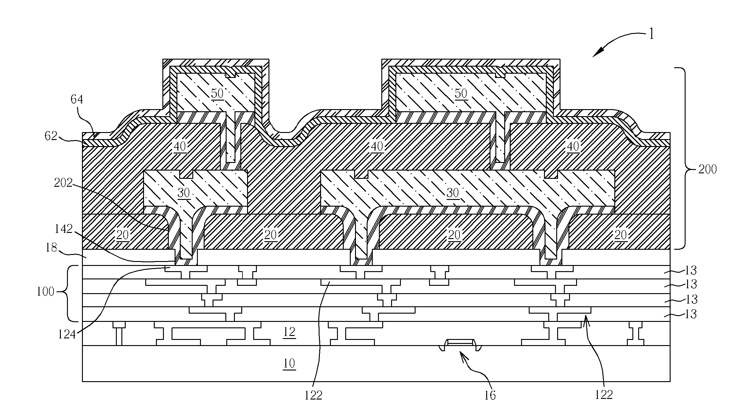
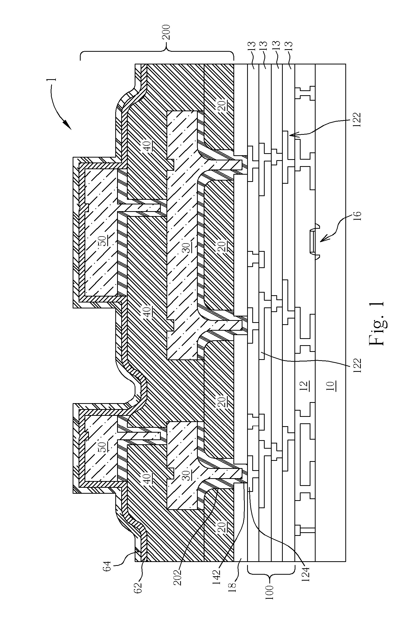
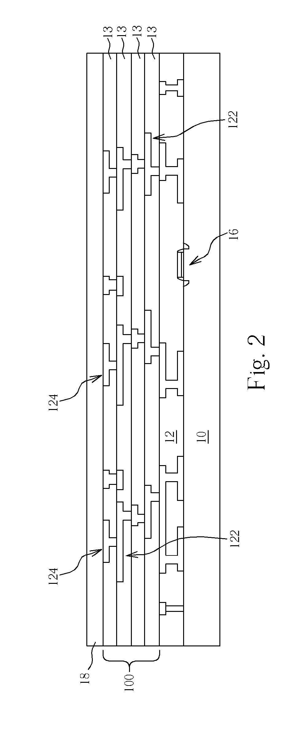
[0022] The present invention discloses a new IC interconnection scheme that is suited for high speed, low power consumption, low voltage, and / or high current IC chips, typically formed on semiconductor wafers. The invention also discloses a post-passivation embossing process, a selective electroplating method to form a thick metal. Incorporating this embossing method, a new interconnection scheme is described, comprising both post-passivation coarse metal interconnection and pre-possivation fine metal interconnection schemes integrated in an IC chip. The coarse metal interconnection, typically formed by selective electroplating technology, is located on top of the fine line interconnection scheme. It is especially useful for long distance lines, clock, power and ground buses, and other applications such as high Q inductors and bypass lines. The fine line interconnections are more appropriate to be used for local interconnections. The combined structure of coarse and fine metal inter...


PUM


Abstract

A new interconnection scheme is described, comprising both coarse and fine line interconnection schemes in an IC chip. The coarse metal interconnection, typically formed by selective electroplating technology, is located on top of the fine line interconnection scheme. It is especially useful for long distance lines, clock, power and ground buses, and other applications such as high Q inductors and bypass lines. The fine line interconnections are suited for local interconnections. The combined structure of coarse and fine line interconnections forms a new interconnection scheme that not only enhances IC speed, but also lowers power consumption.

Description

CROSS REFERENCE TO RELATED APPLICATIONS [0001] This application claims the benefits of U.S. provisional application No. 60 / 684,815, filed May 25, 2005.BACKGROUND OF THE INVENTION [0002] 1. Field of the Invention [0003] The invention relates to the field of high performance integrated circuit devices, and more particularly, to a method of post-passivation processing for the creation of conductive interconnects capable of reducing the parasitic capacitance and resistance of interconnecting wiring on chip. [0004] 2. Description of the Prior Art [0005] Improvements in semiconductor device performance are typically obtained by scaling down the geometric dimensions of the integrated circuits, resulting in a decrease in the cost per die, while at the same time some aspects of semiconductor device performance are improved. The metal connections which connect the integrated circuit to other circuit or system components become of relative more importance and have, with the further miniaturiza...

Claims


Application Information

Patent Timeline
IPC IPC(8): H01L23/48
CPCH01L23/5227H01L2224/0401H01L23/5286H01L23/53238H01L23/53252H01L23/5329H01L2924/09701H01L24/05H01L24/13H01L2224/48463H01L2224/13022H01L2224/02166H01L2224/04042H01L2224/05556H01L23/5283H01L2924/00H01L2924/14H01L2924/15788
Inventor LIN, MOU-SHIUNGCHOU, CHIU-MINGCHOU, CHIEN-KANG
Owner QUALCOMM INC
Why Eureka
Try Eureka