Varactors for CMOS and BiCMOS technologies

Inactive Publication Date: 2005-05-10
IBM CORP
View PDF17 Cites 16 Cited by
  • Summary
  • Abstract
  • Description
  • Claims
  • Application Information

AI Technical Summary

Benefits of technology

[0012]A yet further object of the present invention is to provide varactors which can be easily implemented in existing CMOS and BiCMOS technologies.
[0013]An even further object of the present invention is to provide methods of fabricating varactors which are highly tunable, highly linear and have the highest possible quality factor associated therewith.
[0014]These and other objects and advantages are achieved by providing either a quasi-hyper-abrupt base-collector junction varactor having an Sb (antimony) spike located between the extrinsic base and the subcollector region of a bipolar device; or alternatively, an MOS varactor having a polySi gate and a well region of opposite doping types, i.e., polarity, as well as a subcollector reach-through region to reduce well resistance.

Problems solved by technology

Many of the known prior art varactors do not meet the above criteria.
For example, traditional base-collector junction varactors rely on the NPN base-collector profile, which is not optimized for varactor tunability.
With traditional MOS varactors, the tunability is high; however, an even higher tunability is often required.

Method used


Image

  • Varactors for CMOS and BiCMOS technologies
  • Varactors for CMOS and BiCMOS technologies
  • Varactors for CMOS and BiCMOS technologies

Examples


Embodiment Construction

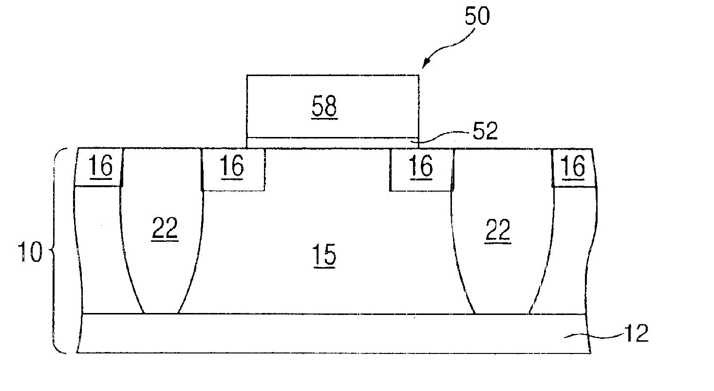
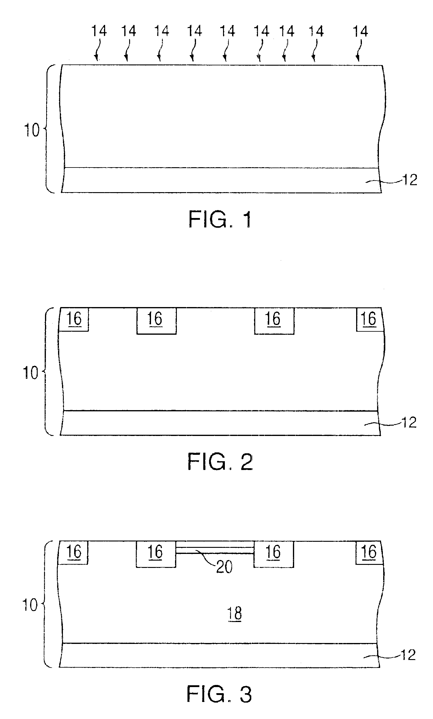
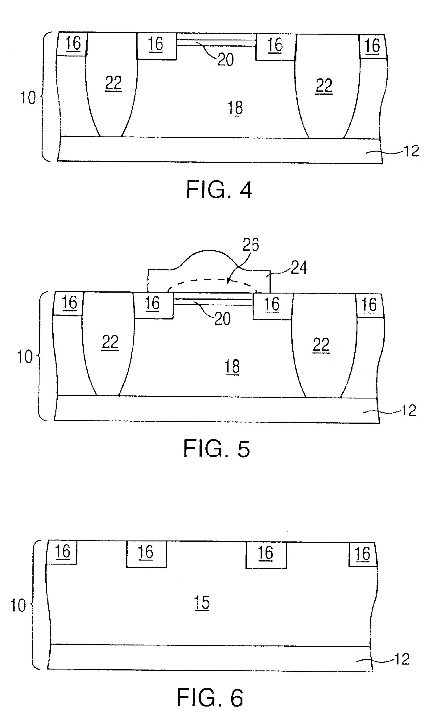
[0035]The present invention, which provides novel varactors for CMOS and BiCMOS technologies as well as methods for fabricating the same, will now be described in more detail by referring to the drawings that accompany the present application.

[0036]Reference is first made to the embodiment illustrated in FIGS. 1-5 wherein the various processing steps employed in fabricating the inventive quasi hyper-abrupt base-collector junction varactor are shown. FIG. 1 illustrates the first step used in forming the inventive quasi hyper-abrupt base-collector junction varactor. Specifically, FIG. 1 shows the formation of subcollector region 12 in a lower portion of substrate 10. The term “substrate” is used herein to denote any semiconductor substrate such as Si, Ge, SiGe, GaAs, InAs, InP, and layered semiconductors such as Si / Si, Si / SiGe and silicon-on-insulators (SOIs). A preferred substrate employed in the present invention is a Si substrate.

[0037]Subcollector region 12 is formed by implanting...


PUM


Abstract

Varactors are provided which have a high tunability and / or a high quality factor associated therewith as well as methods for fabricating the same. One type of varactor disclosed is a quasi hyper-abrupt base-collector junction varactor which includes a substrate having a collector region of a first conductivity type atop a subcollector region, the collector region having a plurality of isolation regions present therein; reach-through implant regions located between at least a pair of the isolation regions; a SiGe layer atop a portion of the substrate not containing a reach-through implant region, the SiGe layer having an extrinsic base region of a second conductivity type which is different from the first conductivity type; and an antimony implant region located between the extrinsic base region and the subcollector region. Another type of varactor disclosed is an MOS varactor which includes at least a poly gate region and a well region wherein the poly gate region and the well region have opposite polarities.

Description

RELATED APPLICATIONS[0001]This application is a divisional of U.S. application Ser. No. 10 / 016,539, filed Dec. 13, 2001, now U.S. Pat. No. 6,521,506.FIELD OF THE INVENTION[0002]The present invention relates to complementary metal oxide semiconductor (CMOS) and bipolar / CMOS (BiCMOS) devices which include a varactor that has improved tunability associated therewith as well as processes for fabricating such devices. The inventive electronic devices, which include the varactor, are highly suitable for use in mobile or cellular phones, personnel digital assistances (PDAs) and other high RF (radio frequency) electronic devices.BACKGROUND OF THE INVENTION[0003]Varactors are electronic devices which have a capacitance that is controlled by a suitable voltage or current bias. Varactors are typically employed, for example, in so-called voltage controlled oscillators (VCOs) where a frequency of an oscillator is controlled by an applied current or voltage. In such instances, the VCOs are used w...

Claims


Application Information

Patent Timeline
IPC IPC(8): H01L29/66H01L27/08H01L29/94H01L29/93H01L21/8222
CPCH01L27/0808H01L29/94H01L29/93H01L27/0811
Inventor COOLBAUGH, DOUGLAS D.DUNN, JAMES S.GORDON, MICHAEL D.HAMMAD, MOHAMMED Y.JOHNSON, JEFFREY B.SHERIDAN, DAVID C.
Owner IBM CORP
Why Eureka
Try Eureka