Method and apparatus for enabling a timing synchronization circuit

a timing synchronization and circuit technology, applied in the direction of pulse automatic control, pulse technique, generating/distributing signals, etc., can solve the problems of large differences in the phases of the respective chip generated clocks, insufficient system reference clocks to all components, and output clock signals jitter

Inactive Publication Date: 2005-05-10
MICRON TECH INC
View PDF9 Cites 25 Cited by
  • Summary
  • Abstract
  • Description
  • Claims
  • Application Information

AI Technical Summary

Problems solved by technology

The improved performance of computing integrated circuits and the growing trend to include several computing devices on the same board present a challenge with respect to synchronizing the time frames of all the components.
While the operation of all components in the system should be highly synchronized, i.e., the maximum skew in time between significant edges of the internally generated clocks of all the components should be minimized, it is not enough to feed the reference clock of the system to all the components.
This is because different chips may have different manufacturing parameters, which, when taken together with additional factors such as ambient temperature, voltage, and processing variations, may lead to large differences in the phases of the respective chip generated clocks.
This undesirable shifting results in jitter in the output clock signal.
This jitter in the output signal may reduce the stability of, or cause an error in, the digital device relying on the output clock.
DDLL circuits typically require a relatively large number of clock cycles to synchronize.
DDLL circuits are also not well suited to handling large temperature or voltage shifts due to their slow response time.
One drawback of such circuits is noise sensitivity, which may result in considerable jitter due to process, voltage, and temperature (PVT) variations.

Method used


Image

  • Method and apparatus for enabling a timing synchronization circuit
  • Method and apparatus for enabling a timing synchronization circuit
  • Method and apparatus for enabling a timing synchronization circuit

Examples


Embodiment Construction

[0019]Illustrative embodiments of the invention are described below. In the interest of clarity, not all features of an actual implementation are described in this specification. It will of course be appreciated that in the development of any such actual embodiment, numerous implementation-specific decisions must be made to achieve the developers' specific goals, such as compliance with system-related and business-related constraints, which will vary from one implementation to another. Moreover, it will be appreciated that such a development effort might be complex and time-consuming, but would nevertheless be a routine undertaking for those of ordinary skill in the art having the benefit of this disclosure.

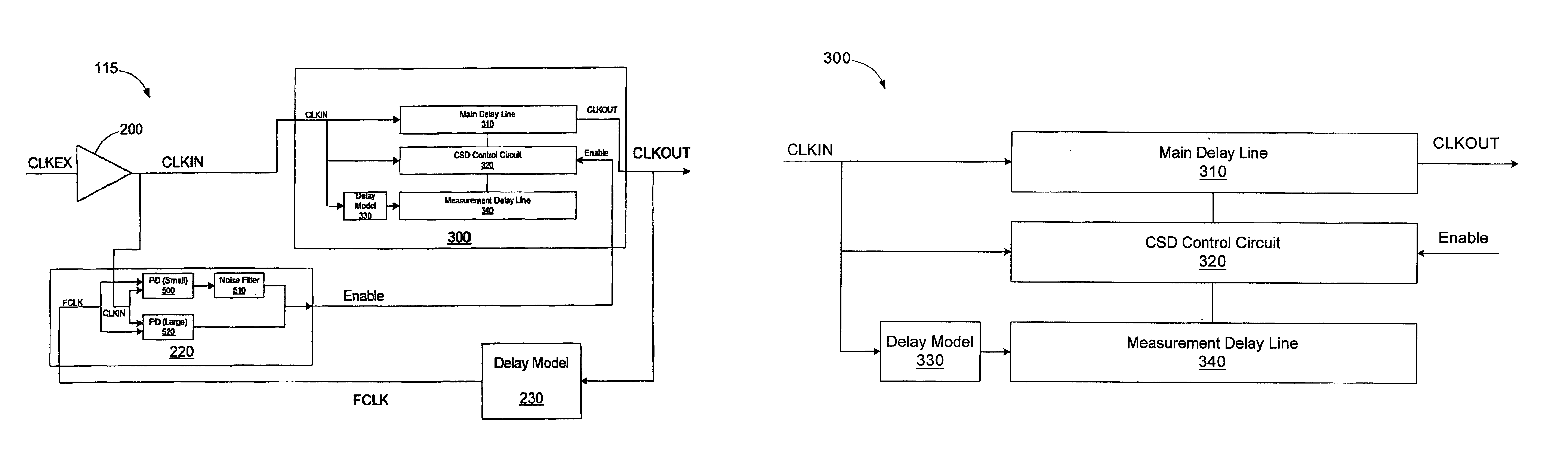
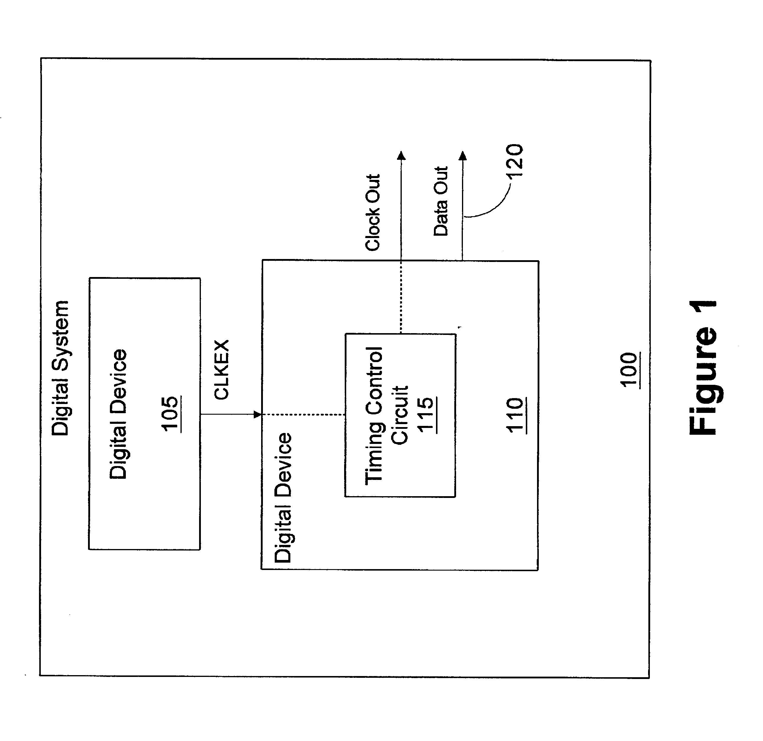
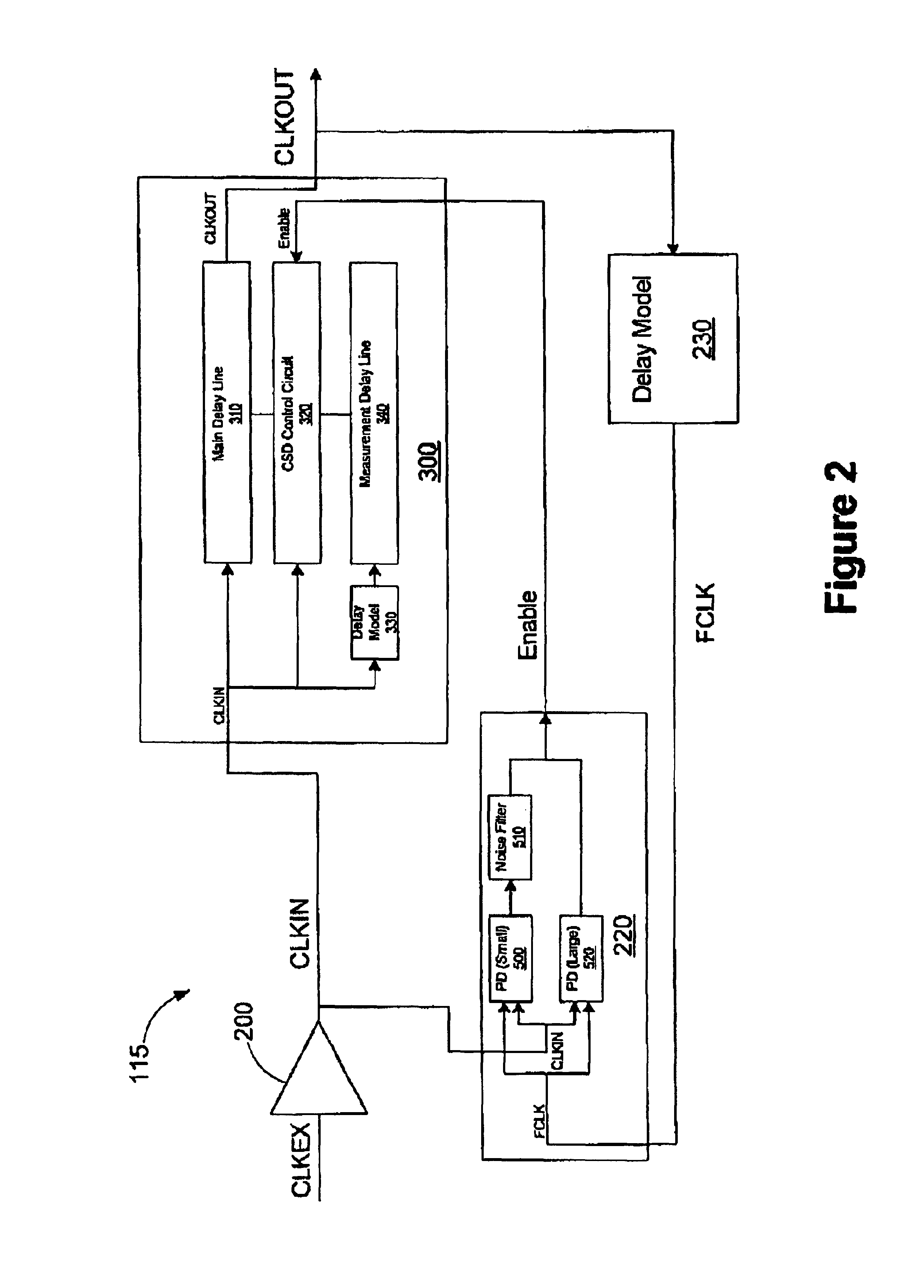
[0020]Referring to FIG. 1, a simplified block diagram of a digital system 100 is provided. The digital system 100 includes a first digital device 105 coupled to a second digital device 110. The first digital device 105 provides a reference clock signal (CLKEX) to the second digit...


PUM


Abstract

A timing control circuit includes a synchronization circuit and a detection circuit. The synchronization circuit includes a main delay line configured to receive an input clock signal and delay the input clock signal by a time interval to generate an output clock signal and a control circuit configured to control the main delay line to vary the time interval to synchronize the input clock signal with a feedback clock signal generated from the output clock signal responsive to assertion of an enable signal. The detection circuit is configured to receive the input clock signal and the feedback clock signal, detect a phase alignment error between the input clock signal and the feedback clock signal, and assert the enable signal responsive to the phase alignment error exceeding a predetermined amount. A method for synchronizing clock signals includes receiving an input clock signal; delaying the input signal by a time interval to generate an output clock signal; controlling the time interval to synchronize the input clock signal with a feedback clock signal generated from the output clock signal responsive to assertion of an enable signal; detecting a phase alignment error between the input clock signal and the feedback clock signal; and asserting the enable signal responsive to the phase alignment error exceeding a predetermined amount.

Description

BACKGROUND OF THE INVENTION[0001]1. Field of the Invention[0002]This invention relates generally to the field of semiconductor device manufacturing and, more particularly, to a method and apparatus for enabling a timing synchronization circuit.[0003]2. Description of the Related Art[0004]Many high speed electronic systems possess critical timing requirements that dictate a need to generate a periodic clock waveform possessing a precise timing relationship with respect to some reference signal. The improved performance of computing integrated circuits and the growing trend to include several computing devices on the same board present a challenge with respect to synchronizing the time frames of all the components.[0005]While the operation of all components in the system should be highly synchronized, i.e., the maximum skew in time between significant edges of the internally generated clocks of all the components should be minimized, it is not enough to feed the reference clock of the...

Claims


Application Information

Patent Timeline
Patent Type & Authority Patents(United States)
IPC IPC(8): H03K5/135H03L7/00
CPCH03L7/00H03K5/135G06F1/10G11C7/22G11C7/222H03L7/0812H03L7/0814
Inventor MIKHALEV, VLADIMIRLIN, FENG
Owner MICRON TECH INC
Why Eureka
Try Eureka