Multi-channel wavelength division multiplexing using photonic crystals

a technology of photonic crystals and wavelength division, applied in the field of photonic crystals, can solve the problems of not maximizing the utilization of the available bandwidth of the photonic crystals, and maximizing the density of frequency-selective channels

Inactive Publication Date: 2005-05-10
UNIVERSITY OF DELAWARE
View PDF1 Cites 12 Cited by
  • Summary
  • Abstract
  • Description
  • Claims
  • Application Information

AI Technical Summary

Benefits of technology

[0010]The present invention satisfies this need by providing a multi-channel WDM device made from photonic crystals having a bank of high Q-value microcavities tuned to different frequencies.

Problems solved by technology

These conventional WDM devices fail to maximize the density of frequency-selective channels, and thus, fail to maximize usage of the available bandwidth of the photonic crystals.

Method used


Image

  • Multi-channel wavelength division multiplexing using photonic crystals
  • Multi-channel wavelength division multiplexing using photonic crystals
  • Multi-channel wavelength division multiplexing using photonic crystals

Examples


Embodiment Construction

[0023]Reference will now be made in detail to the present preferred embodiment of the invention, an example of which is illustrated in the accompanying drawings. Wherever possible, the same reference numbers will be used throughout the drawings to refer to the same or like parts.

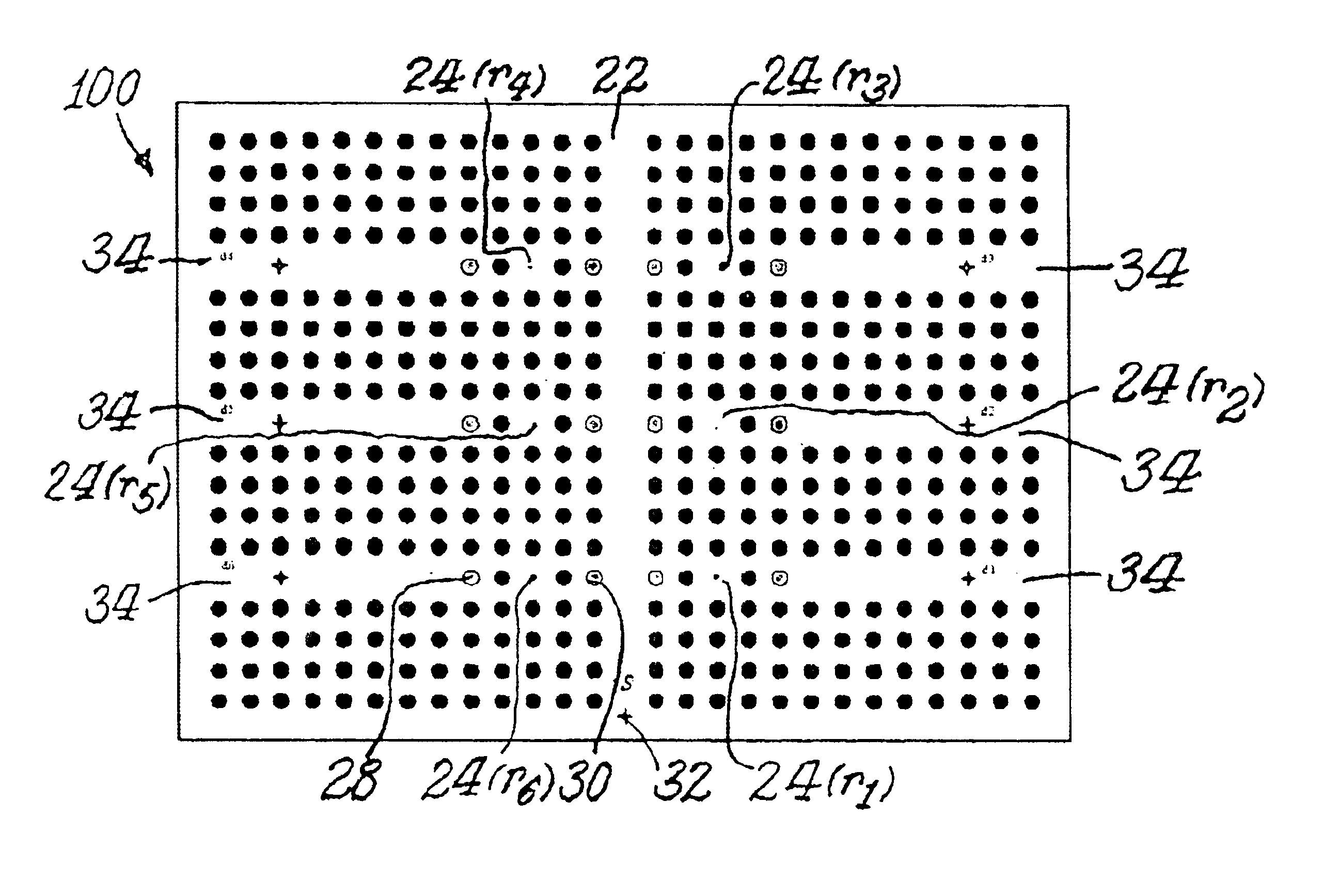
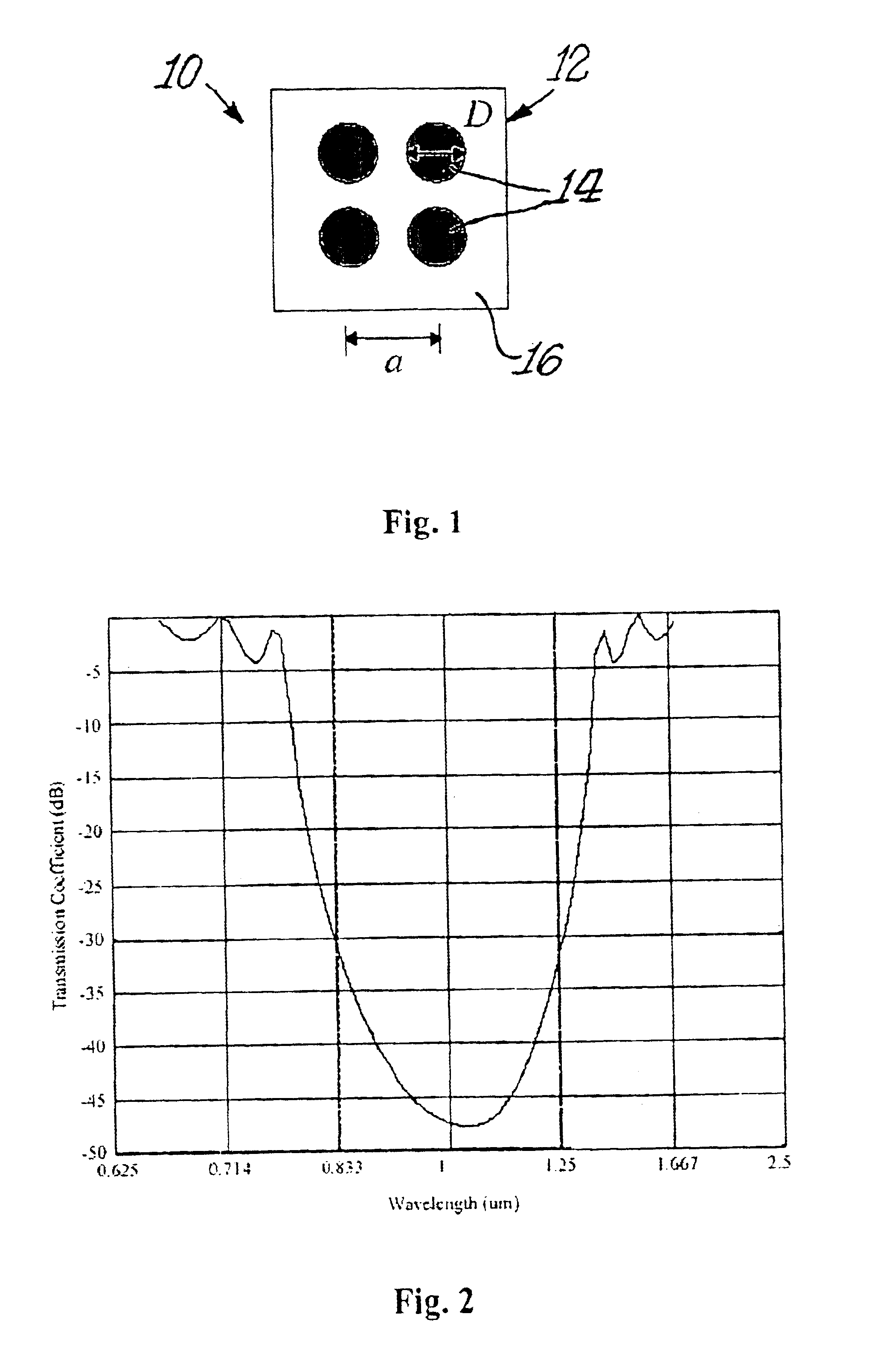
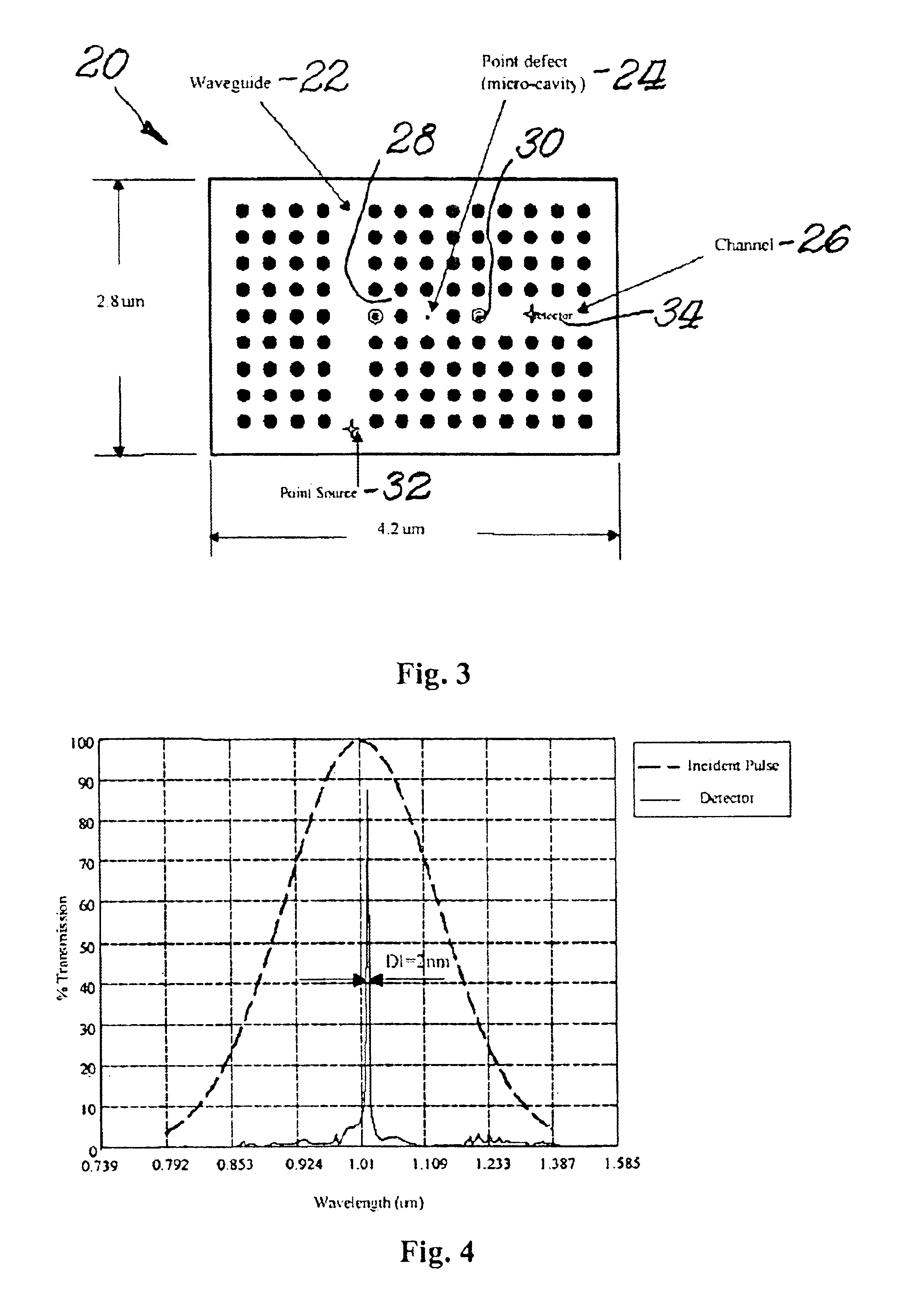
[0024]A. Localization of Light in Photonic Crystals

[0025]The physical phenomena that clearly describes the operation of a photonic crystal is the localization of light, which is achieved from the scattering and interference produced by a coherent wave in a periodic structure. In this case a photon located in a lossless dielectric media provides an ideal realization of a single excited state in a static medium at room temperature. To describe this phenomenon, Maxwell's equations are cast into a form similar to Schrodinger's to produce the following Equation (1): ∇×(∇×E⁡(r))=(ωc)2⁢ɛ⁡(r)⁢E⁡(r),(1)

where E(r) is the electric field, ω is the angular frequency, c is the ∈(r) is the dielectric function, and r is the...


PUM


Abstract

Described herein is a multi-channel wavelength division multiplexing (WDM) device including a two-dimensional photonic crystal. The photonic crystal consists of two primary components: (1) a waveguiding element created by line defects formed in the photonic crystal, and (2) frequency-selective elements created by high Q-value microcavities formed in the crystal. The multi-channel WDM system offers a flexible design and high channel density.

Description

CLAIM FOR PRIORITY[0001]The present application claims priority of U.S. Provisional Patent Application Ser. No. 60 / 297,389, filed Jun. 11, 2001 the disclosure of which being incorporated by reference herein in its entirety.BACKGROUND OF THE INVENTION[0002]A. Field of the Invention[0003]The present invention relates generally to photonic crystals, and, more particularly to multi-channel wavelength division multiplexing using photonic crystals.[0004]B. Description of the Related Art[0005]During the last decade photonic crystals (also known as photonic band-gap materials) have risen from an obscure technology to a prominent field of research. In large part this is due to their unique ability to control, or redirect, the propagation of light. E. Yablonovich, “Inhibited spontaneous emission in solid-state physics and electronics,”Physical Review Letters, vol. 58, pp. 2059-2062 (May 1987), and S. John, “Strong localization of photons in certain disordered dielectric superlattices,”Physica...

Claims


Application Information

Patent Timeline
Patent Type & Authority Patents(United States)
IPC IPC(8): G02B6/122G02B6/34G02B6/42
CPCB82Y20/00G02B6/1225G02B6/12007G02B6/4214
Inventor PRATHER, DENNIS W.SHARKAWY, AHMEDSHI, SHOUYUN
Owner UNIVERSITY OF DELAWARE
Why Eureka
Try Eureka