Trench gate semiconductor device and the method of manufacturing the same

a technology of trench gate semiconductor and trench gate, which is applied in the direction of semiconductor devices, basic electric elements, electrical apparatus, etc., can solve the problems of low contact resistance between the source region surface and the source electrode, affecting the ability of the avalanche to stand up to the force, and difficult control of the manufacturing process, etc., to achieve the effect of reducing the body resistance of the parasitic bjt therein and facilitating the increase of channel density

Inactive Publication Date: 2011-06-30
FUJI ELECTRIC CO LTD
View PDF5 Cites 6 Cited by
  • Summary
  • Abstract
  • Description
  • Claims
  • Application Information

AI Technical Summary

Benefits of technology

[0040]According to the invention, a semiconductor device that facilitates increasing the

Problems solved by technology

Since the parasitic BJT is liable to be turned off, when an avalanche breakdown is caused between the drift region and the n+ source region, the avalanche withstanding capability is liable to be low.
Since it is

Method used


Image

  • Trench gate semiconductor device and the method of manufacturing the same
  • Trench gate semiconductor device and the method of manufacturing the same
  • Trench gate semiconductor device and the method of manufacturing the same

Examples


Embodiment Construction

[0060]Now the invention will be described in detail below with reference to the accompanied drawings which illustrate the preferred embodiments of the invention. Although the invention will be described in connection with the embodiments thereof, changes and modifications are obvious to the persons skilled in the art without departing from the true spirit of the invention. Therefore, the invention will be defined by the appended claims.

Structure

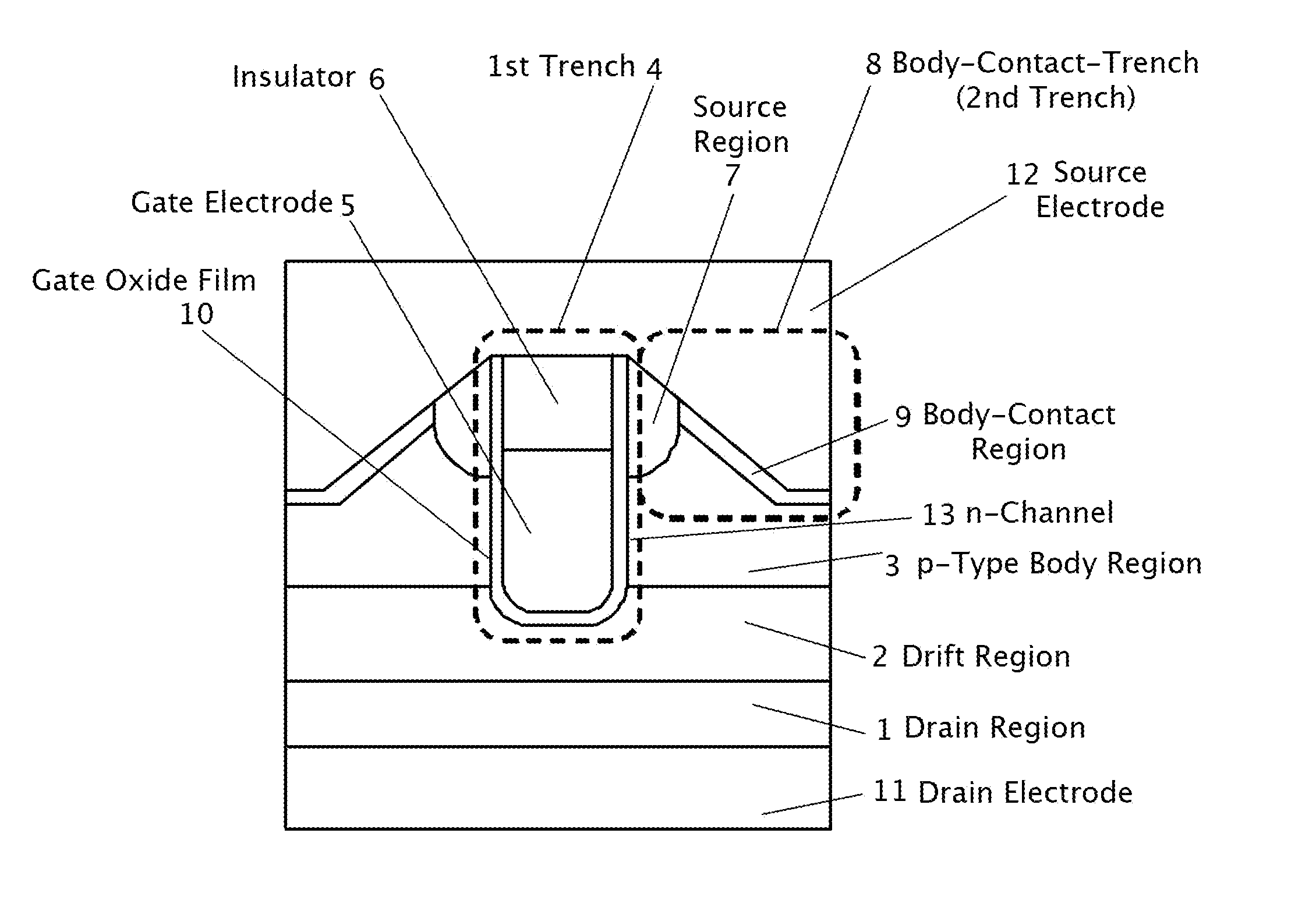
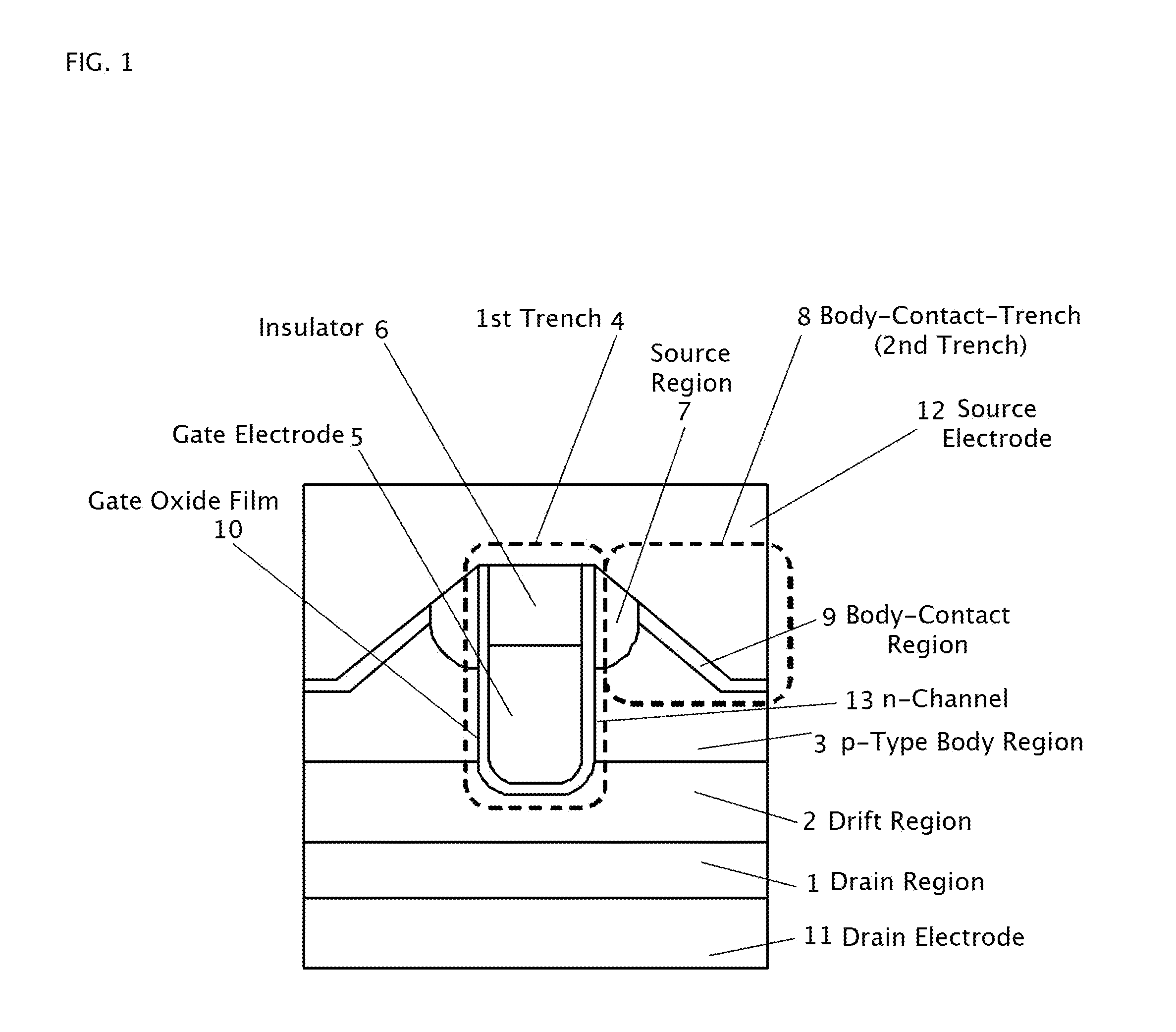
[0061]FIG. 1 is the cross sectional view of a trench gate MOSFET according to the invention. Referring now to FIG. 1, lightly doped n-type drift region 2 is formed on a heavily doped n-type silicon substrate that works for drain region 1. Lightly doped p-type body region 3 is formed on n-type drift region 2. A plurality of first trenches 4 are formed selectively from the surface of p-type body region 3. Each first trench 4 is extended into n-type drift region 2. Polysilicon that works for gate electrode 5 is loaded in the lower portion of eac...


PUM


Abstract

A trench gate semiconductor device is disclosed which has a trench gate structure including an insulator in the upper portion of a first trench, the insulator being on a gate electrode; a source region having a lower end surface positioned lower than the upper surface of the gate electrode; a second trench in the surface portion of a semiconductor substrate between the first trenches, the second trench having a slanted inner surface providing the second trench with the widest trench width at its opening and a bottom plane positioned lower than the lower end surface of the source region, the slanted inner surface being in contact with the source region; and a p-type body-contact region in contact with the slanted inner surface of the second trench. The trench gate semiconductor device and its manufacturing method facilitate increasing the channel density and lowering the body resistance of the parasitic BJT.

Description

BACKGROUND OF THE INVENTION[0001]A. Field of the Invention[0002]The present invention relates to MOS semiconductor devices used in switching power supplies. Specifically, the invention relates to trench gate semiconductor devices and the method of manufacturing the trench gate semiconductor devices. More specifically, the invention relates to a trench gate MOSFET including a source region and a contact-trench formed by self-alignment or a trench gate IGBT including a source region and a contact-trench formed by self-alignment. More specifically, the invention relates also to the method of manufacturing the trench gate MOSFET or the trench gate IGBT.[0003]B. Description of the Related Art[0004]Generally, it is required for the semiconductor devices used in switching power supplies to sustain the voltage applied thereto in the OFF-state and to exhibit low resistance (low ON-state resistance) against the current made to flow in the ON-state of the semiconductor devices. In the low-volt...

Claims


Application Information

Patent Timeline
IPC IPC(8): H01L29/78H01L29/739H01L21/336
CPCH01L21/26586H01L29/1095H01L29/41766H01L29/66348H01L29/66666H01L29/66734H01L29/7397H01L29/7813H01L29/66727
Inventor IKURA, YOSHIHIRO
Owner FUJI ELECTRIC CO LTD
Why Eureka
Try Eureka