
Power semiconductor device with L shaped source

A power semiconductor and source region technology, applied in semiconductor devices, electrical components, circuits, etc., can solve the problems of reduced breakdown voltage, affecting the channel, inability to control the threshold voltage, etc., to achieve increased channel density and reduced cellpitch. Effect

Inactive Publication Date: 2006-11-15
ONIZUKA ELECTRONICS
View PDF0 Cites 2 Cited by
  • Summary
  • Abstract
  • Description
  • Claims
  • Application Information

AI Technical Summary

Problems solved by technology

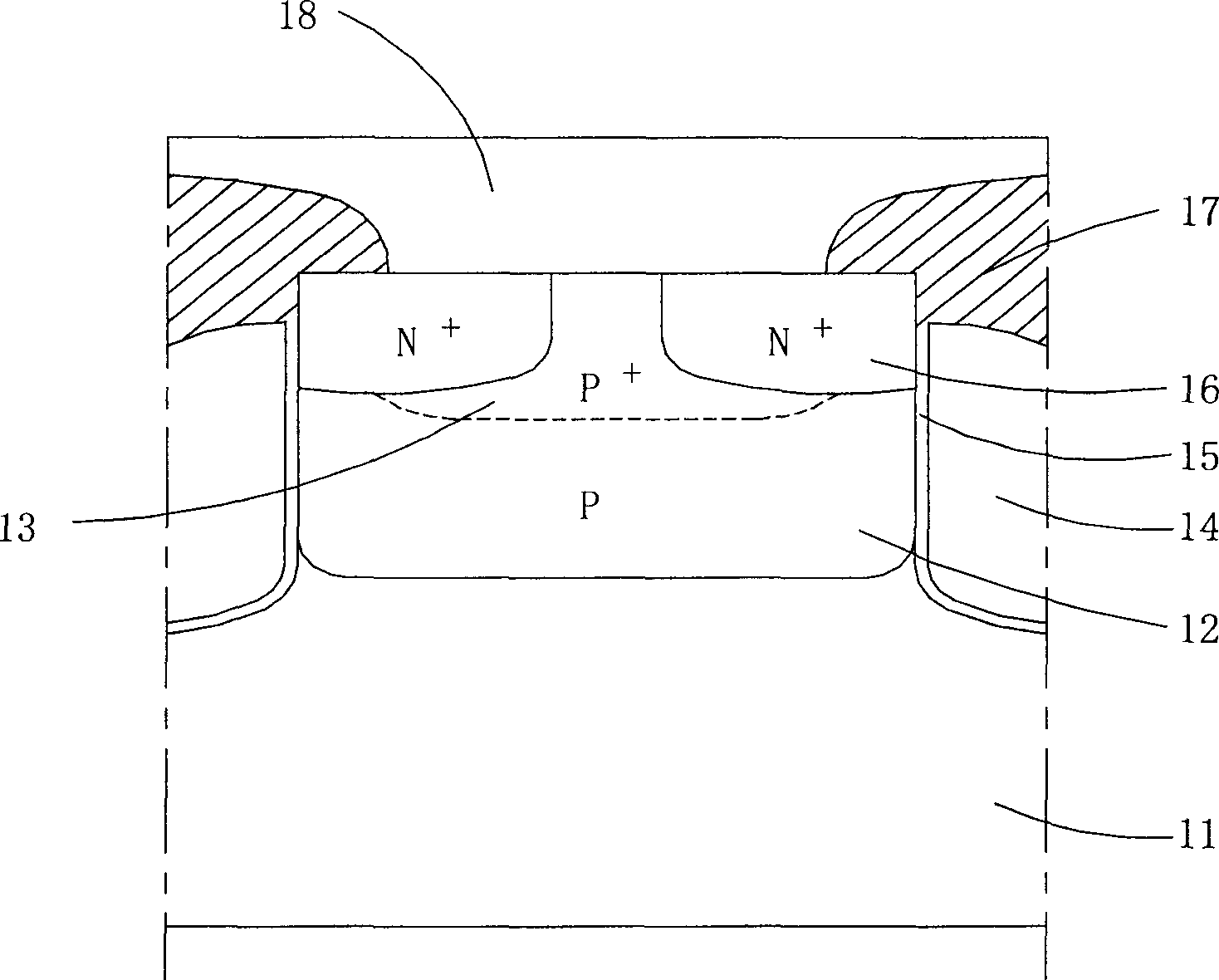
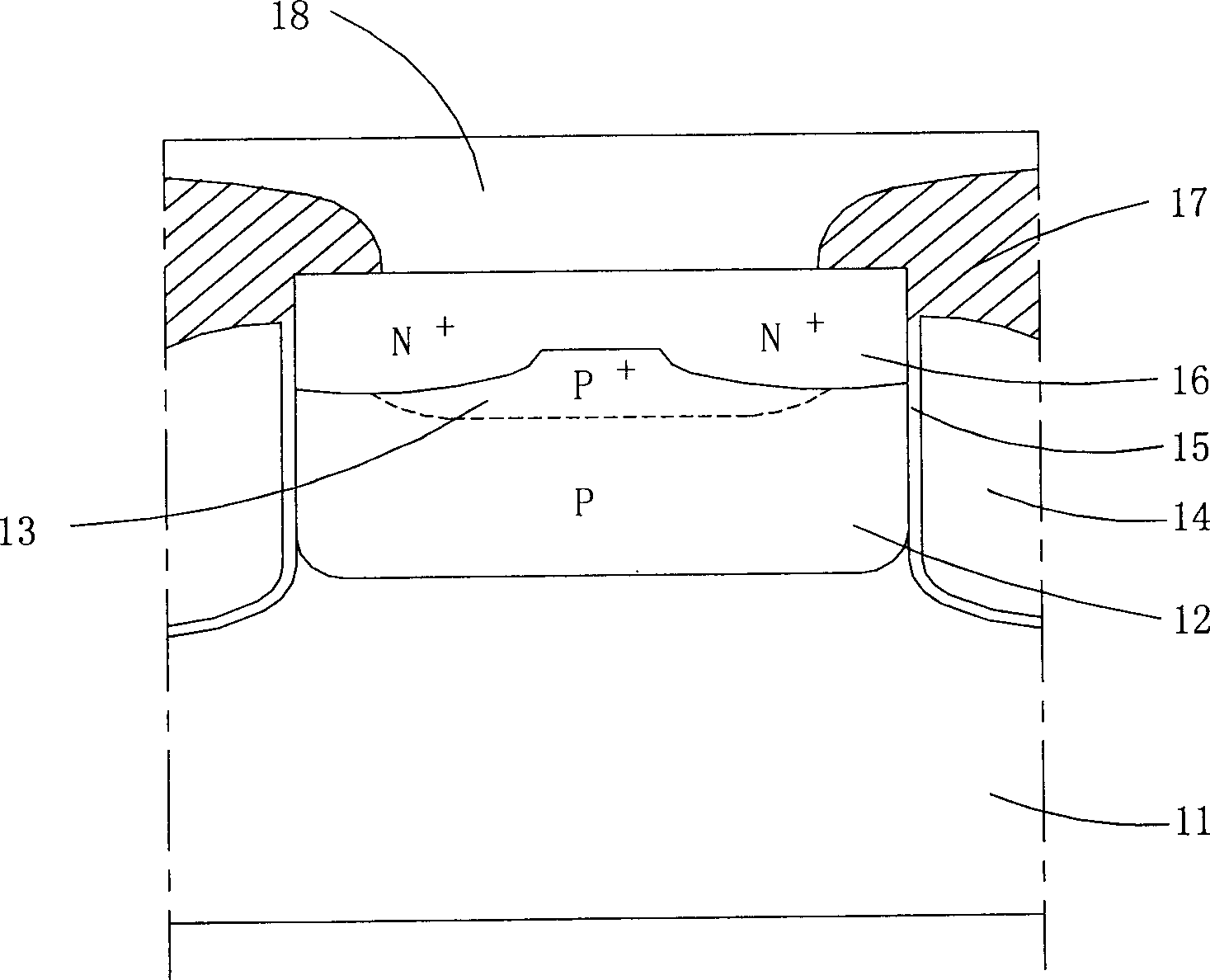
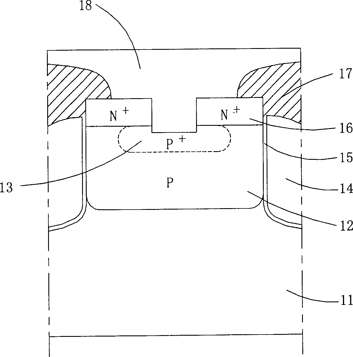
First, since the P+ type body region 13 is deeper than the N+ type source region 16, the channel region is exposed to the P+ type body region 13, and the dopant in the P+ region will easily enter the channel, resulting in a high and uncontrollable channel region. The threshold voltage (threshold voltage)
On the other hand, the deeply implanted P+ type body region 13 will limit the depletion region distribution in the P+ region
Therefore, when the depth of the P+ type body region 13 increases, the breakdown voltage (breakdown voltage) of the device will be limited or even reduced.
[0006] In view of known power semiconductor devices, the breakdown voltage (breakdown voltage) will be limited or even reduced due to the depth of the body region, and the threshold voltage (threshold voltage) will also be affected by the dopant in the P+ type region structure. Channel, As a result, the electrical properties of the overall device are affected

Method used


Image

  • Power semiconductor device with L shaped source
  • Power semiconductor device with L shaped source
  • Power semiconductor device with L shaped source

Examples


Embodiment Construction

[0053] Some typical embodiments embodying the features and advantages of the present invention will be described in detail in the following description. It should be understood that the present invention can have various changes in different aspects, all without departing from the scope of the present invention, and the description and drawings therein should be used for illustration in nature, rather than for limiting the invention .

[0054] see Figure 4 , which discloses a buried trench gate power semiconductor device structure with an L-shaped source region according to a preferred embodiment of the present invention. As shown in the figure, the structure of the buried trench gate power semiconductor device with L-shaped source region of the present invention mainly includes a substrate 21, a well region 22, a body region 23, a trench gate 24, and a gate oxide layer. 25 , L-shaped source region 26 , dielectric insulating layer 27 and metal layer 29 . The well region 22...


PUM


Abstract

This invention relates to L type source region power semiconductor device. It includes one substrate, one trap area formed in the substrate, one body area formed on trap area, one groove grid formed at both sides of the trap area, one grid oxide layer is formed on the lateral wall and bottom surface of the groove grid, one L type source region, and one flat roof area and one straight lateral area are formed on roof and sides of the body, one dielectric insulating layer formed on the groove grid area and part of the L type area, and one contact window is defined, one metal layer formed on the insulating layer, the body and the L type area, and it is connected to the L type area through the contact window to form the power semiconductor device with L type area flush type groove grid.

Description

technical field [0001] The present invention relates to a power semiconductor device structure, in particular to a power semiconductor device structure with an L-shaped source region. Background technique [0002] In recent years, power semiconductor devices, such as metal oxide semiconductor field effect transistor (MOSFET), insulated gate bipolar transistor (IGBT), junction field effect transistor (Junction FieldEffect Transistor, JFET) or rectifier diodes (Rectifier), etc., have made extremely good progress in their operational performance and manufacturing process. However, in order to further improve the characteristics of the device and reduce the manufacturing cost, one of the main trends is to use the so-called trench-gated technology. However, when using this trench gate technology, the cell pitch of the device is reduced, and the device channel density of the device is significantly increased. Such a low on-state power loss can be achieved by forming low on-resis...

Claims


Application Information

Patent Timeline
Patent Type & Authority Applications(China)
IPC IPC(8): H01L29/78H01L29/772
Inventor 曾军孙伯益
Owner ONIZUKA ELECTRONICS
Learn More