Trench gate super-barrier rectifier

A super-barrier rectifier and trench gate technology, applied in semiconductor devices, electrical components, circuits, etc., can solve the problems of large channel resistance, large cell size, and difficult process, and achieve small channel resistance and repeatability. The effect of good performance and simple process

Inactive Publication Date: 2019-06-11
GUIZHOU E CHIP MICROELECTRONICS TECH CO LTD
View PDF6 Cites 2 Cited by
  • Summary
  • Abstract
  • Description
  • Claims
  • Application Information

AI Technical Summary

Problems solved by technology

[0005] The invention provides a trench gate super-barrier rectifier, which solves the problem of relatively large cell size, relatively large channel resistance, relatively low reliability, and relatively large process difficulty in the existing planar gate super-barrier rectifier. and other shortcomings

Method used


Image

  • Trench gate super-barrier rectifier
  • Trench gate super-barrier rectifier
  • Trench gate super-barrier rectifier

Examples


Embodiment Construction

[0044] Below in conjunction with specific embodiment of the present invention and accompanying drawing, the preparation method of the present invention is described in detail:

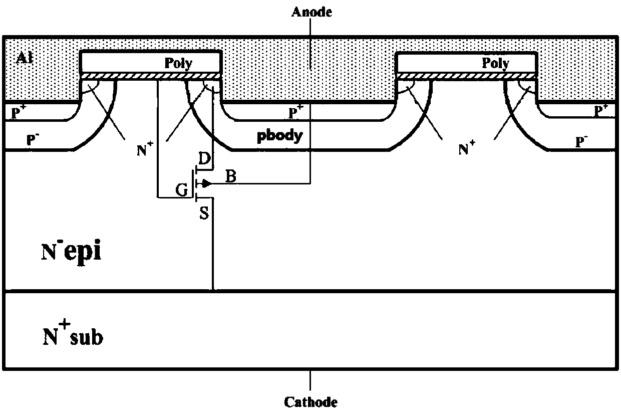
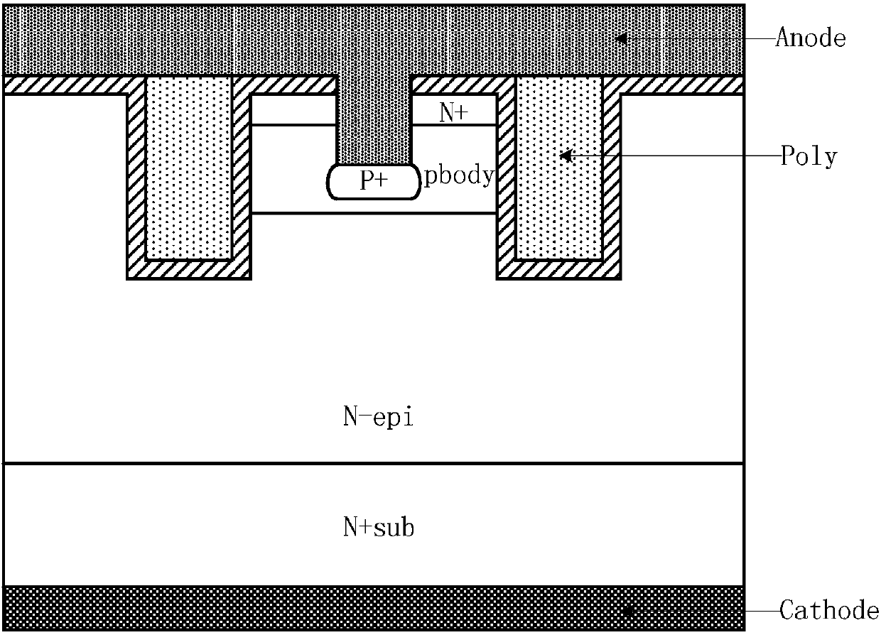
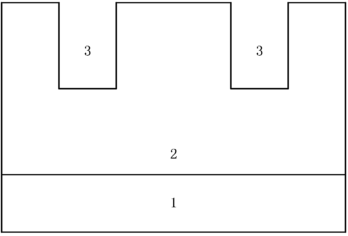
[0045] Figure 3(a)~Figure 3(h) Shown is the flow chart of making the trench gate super-barrier rectifier in this embodiment, and each step is described one by one below:

[0046] Step A: growing an N-type epitaxial layer 2 on an N-type substrate 1, and then performing etching in the N-type epitaxial layer 2 to form a trench 3, as shown in FIG. 3(a). According to common knowledge in the field, it can be known that the N-type substrate 1 is heavily doped, and the N-type epitaxial layer 2 is lightly doped. The specific doping concentration is based on the prior art and can be selected according to actual requirements, so it will not be repeated here. In this embodiment, the longitudinal cross-sectional shape of the trench 3 is a rectangle. According to common knowledge in the field, the depth of the tre...


PUM


Abstract

The invention provides a trench gate super-barrier rectifier, and belongs to the technical field of semiconductor power devices; the improvement of an existing super-barrier rectifier is as follows: atrench gate structure is adopted to replace a plane gate structure; on one hand, the cell size of the trench gate super-barrier rectifier is small, and the channel resistance is low; on the other hand, a gate oxide layer is located below the surface of a silicon wafer, so that damage to a lead bonding process is avoided, and the reliability is improved; and in addition, a channel region can be formed by adopting a conventional ion implantation method, so that the repeatability and the yield are high.

Description

technical field [0001] The invention belongs to the technical field of semiconductor power devices, and in particular relates to a trench gate super-barrier rectifier. Background technique [0002] The super-barrier rectifier is a new type of two-terminal power electronic device. It combines the advantages of two conventional rectifiers, PIN tube and Schottky tube, and has the advantages of low turn-on voltage, small reverse leakage, good reverse recovery characteristics, and high reliability. [0003] The super-barrier rectifier is similar to a VDMOS with a gate-drain short circuit, and its minority carrier barrier is generated by the MOS channel formed by the N+ drain region, Pbody and N- epitaxial layer. When the positive voltage is applied to the anode, it is equivalent to that the gate and drain of the MOS are connected to a high potential at the same time, and the source is grounded. Due to the body effect, when the pbody is connected to a high potential, the thresho...

Claims


Application Information

Patent Timeline
Patent Type & Authority Applications(China)
IPC IPC(8): H01L29/10H01L29/423
Inventor 李泽宏钟子期
Owner GUIZHOU E CHIP MICROELECTRONICS TECH CO LTD
Why Eureka
Try Eureka