VDMOS device and manufacturing method thereof

A manufacturing method and device technology, applied in semiconductor/solid-state device manufacturing, semiconductor devices, electrical components, etc., can solve the problems of increasing manufacturing cost and increasing process difficulty, so as to improve performance, reduce source contact resistance, increase The effect of contact area

Inactive Publication Date: 2015-09-16
PEKING UNIV FOUNDER GRP CO LTD +1
View PDF6 Cites 6 Cited by
  • Summary
  • Abstract
  • Description
  • Claims
  • Application Information

AI Technical Summary

Problems solved by technology

Since the contact resistance of the trench VDMOS is composed of two parts, the drain contact resistance and the source contact resistance, now the drain contact resistance is usually reduced by back thinning, back injection, back electrode structure and other process improvements, while the source The contact resistance is mainly improved through the design of the device structure, such as the optimization design of the epitaxial structure and the electrode structure. However, these methods have problems such as increasing the difficulty of the process and increasing the manufacturing cost.

Method used


Image

  • VDMOS device and manufacturing method thereof
  • VDMOS device and manufacturing method thereof
  • VDMOS device and manufacturing method thereof

Examples


Embodiment

[0045] Such as Figure 1 to Figure 10 As shown, the manufacturing method of a VDMOS device according to an embodiment of the present invention includes the following steps:

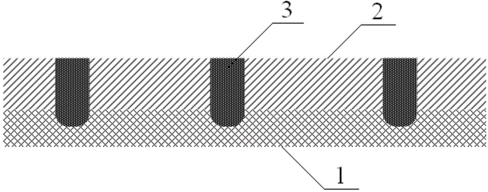
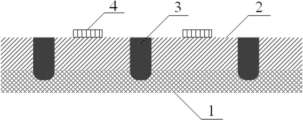
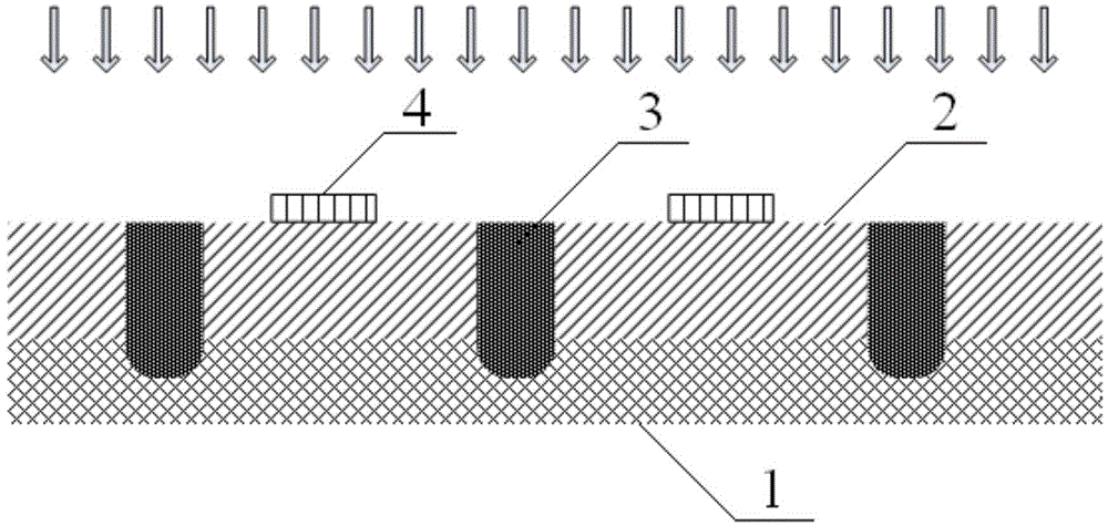
[0046] Step 1, forming a gate trench inside the epitaxial layer of the silicon substrate;

[0047] Specifically, the silicon substrate may be a conventional silicon substrate with an epitaxial layer 1 in the art, such as an epitaxial wafer, or the epitaxial layer 1 may be grown on the silicon substrate by a conventional method in the art;

[0048]First, a gate trench mask (ie, a mask layer with a gate trench pattern) can be formed on the epitaxial layer 1, and then the silicon substrate is etched using the mask to form a gate trench inside the epitaxial layer 1. The gate trench, the gate trench can be a plurality of trenches distributed at intervals, for example, an initial oxide layer can be formed on the epitaxial layer 1 as a mask layer, and then by photolithography and etching, on the initial oxide la...


PUM


Abstract

The invention provides a VDMOS device and a manufacturing method thereof. The manufacturing method comprises the following steps that: a gate oxide layer is formed in gate trenches of a silicon substrate, and the gate trenches of the silicon substrate are filled with polycrystalline silicon; a body region is formed; first ions and second ions are sequentially injected into the silicon substrate, and the silicon substrate is subjected to annealing treatment, and therefore, source contact regions can be formed at two sides of each gate trench, and the first ions and the second ions have the same type, and the energy of the first ions is larger than that of the second ions, and the dosage of the first ions is smaller than that of the second ions; a dielectric layer is formed; after a source trench mask is formed on the dielectric layer, and the silicon substrate is etched, and therefore, source trenches can be formed between the source contact regions; and the source trench mask is removed, and a metal layer is formed on the silicon substrate. With the manufacturing method provided by the invention adopted, the contact resistance of the VDMOS device can be decreased without changing the structure of the device, increasing the manufacturing process difficulty of the device and increasing the manufacturing cost of the device, and therefore, the performance of the device can be improved.

Description

technical field [0001] The invention belongs to the technical field of semiconductors, and in particular relates to a VDMOS device and a manufacturing method thereof. Background technique [0002] Vertical double-diffused metal-oxide semiconductor field-effect transistors (VDMOS) include planar VDMOS and trench VDMOS. Trench VDMOS is a power device with a wide range of uses. Its drain and source poles are arranged on both sides of the device, and the current flows vertically inside the device, thereby increasing the current density and improving the rated current. The on-resistance per unit area is relatively low. Small. [0003] Conventional trench-type VDMOS manufacturing methods generally include forming a gate trench inside the epitaxial layer of a silicon substrate, forming a gate oxide layer and polysilicon inside the gate trench, and then performing ion implantation to form a gate trench inside the epitaxial layer. Then implant different types of ions to form source...

Claims


Application Information

Patent Timeline
Patent Type & Authority Applications(China)
IPC IPC(8): H01L29/78H01L29/423H01L21/336
CPCH01L29/7809H01L21/266H01L29/0865H01L29/66734H01L29/7813
Inventor 李理马万里赵圣哲
Owner PEKING UNIV FOUNDER GRP CO LTD
Why Eureka
Try Eureka