Split-gate flash memory, method of fabricating same and method for control thereof

a technology control method, which is applied in the field of semiconductor technology, can solve the problems of affecting the mass production of split-gate flash memory, increasing channel leakage current, and a considerable short-channel effect, and achieves the effect of reducing the word line-floating gate coupling ratio, and reducing the channel resistan

Active Publication Date: 2019-11-21
SHANGHAI HUAHONG GRACE SEMICON MFG CORP
View PDF11 Cites 6 Cited by
  • Summary
  • Abstract
  • Description
  • Claims
  • Application Information

AI Technical Summary

Benefits of technology

[0010]In order to overcome the above deficiencies of the conventional split-gate flash memory, the present invention proposes a split-gate flash memory, a method of fabricating the split-gate flash memory and a method for control thereof, which mainly offer the advantages as follows: 1) a thinner word-line oxide layer and hence a lower channel resistance; 2) short-channel effect suppression; and 3) a lower word line-floating gate coupling ratio that allow higher erasing efficiency.
[0025]In the split-gate flash memory provided in the present invention, as the word-line structure is constructed on the semiconductor substrate between the first memory region and the second memory region as a stack of the word-line oxide layer, the read gate, the dielectric oxide layer and the erase gate, each of the read and erase gates can function as a word line for the split-gate flash memory to enable a read or erase operation. Compared to conventional split-gate flash memories (e.g., that of FIG. 1), the word-line oxide layer can be made thinner. As a result, during the erase operation, a lower voltage is allowed to be applied to the read gate, which can reduce a channel resistance induced by the word-line structure. Moreover, the read gate is also thinner, which can lower or even eliminate a word line-induced barrier, thereby achieving leakage current suppression and short-channel effect suppression.
[0026]In addition, in the split-gate flash memory provided in the present invention, since the word line depends only in part on the erase gate, compared to conventional devices, the split-gate flash memory of the invention has a lower erase gate-floating gate coupling ratio and thus requires a lower erase gate-floating gate coupling voltage, which can result in a stronger electric field and improved erasing efficiency.
[0028]In the method of fabricating the split-gate flash memory provided in the present invention, during the formation of the word-line structure, the read gate and the erase gate for enabling read and erase operations are stacked together and isolated from each other. This is helpful in channel leakage suppression in the underlying semiconductor substrate when a high voltage is applied to the erase gate during the erase operation. Accordingly, the word-line oxide layer may be made thinner, reducing the required word-line reading voltage and hence a channel resistance induced by the word-line structure. Moreover, the dielectric oxide layer may be formed between the first memory bit structure and the erase gate and between the second memory bit structure and the erase gate so as to provide a tunneling oxide layer between the first floating gate and the erase gate and between the second floating gate and the erase gate.
[0029]In the method for control of the above split-gate flash memory, read and erase operations are enabled by the read and erase gates that are independent from each other, thus helping in channel leakage suppression when a high voltage is applied to the word line during the erase operation. In addition, a lower word-line reading voltage is required because of the reduced word-line oxide layer thickness, which is conducive to short-channel effect suppression. Further, a window between the states in which the read and erase operations are performed can be expanded, which is favorable to mass production.
[0030]Since the split-gate flash memory can be respectively made and controlled by the above methods, they offer the same or analogous advantages.

Problems solved by technology

Additionally, the coupling between the word line 104 and the floating gate 107 can lower a word line-induced barrier, causing increased channel leakage currents and a considerable short-channel effect.
This may hinder the mass production of the split-gate flash memory.

Method used


Image

  • Split-gate flash memory, method of fabricating same and method for control thereof
  • Split-gate flash memory, method of fabricating same and method for control thereof
  • Split-gate flash memory, method of fabricating same and method for control thereof

Examples


Embodiment Construction

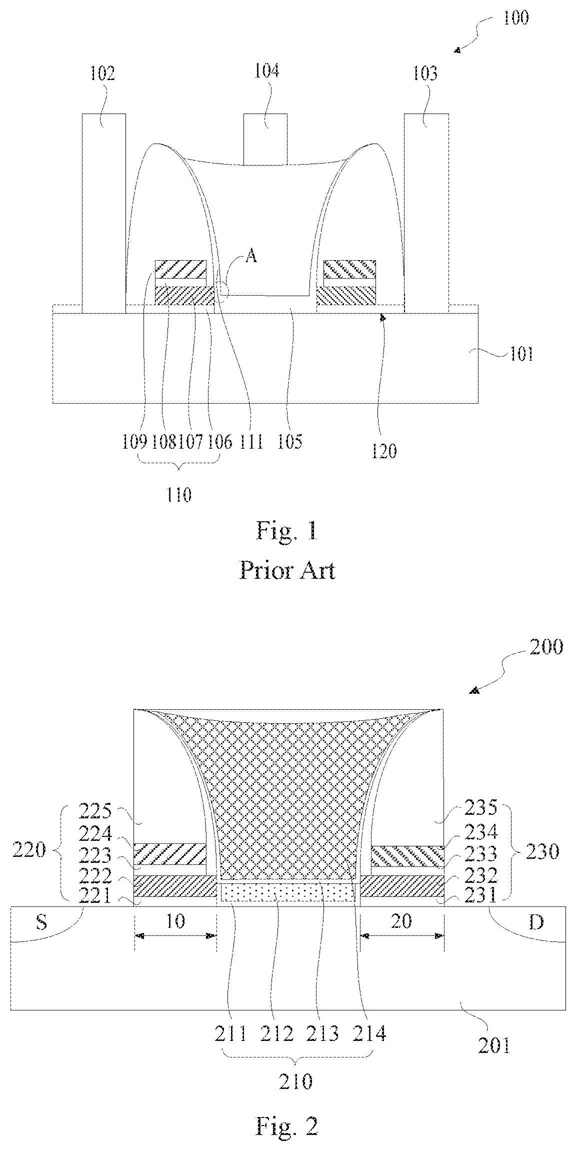
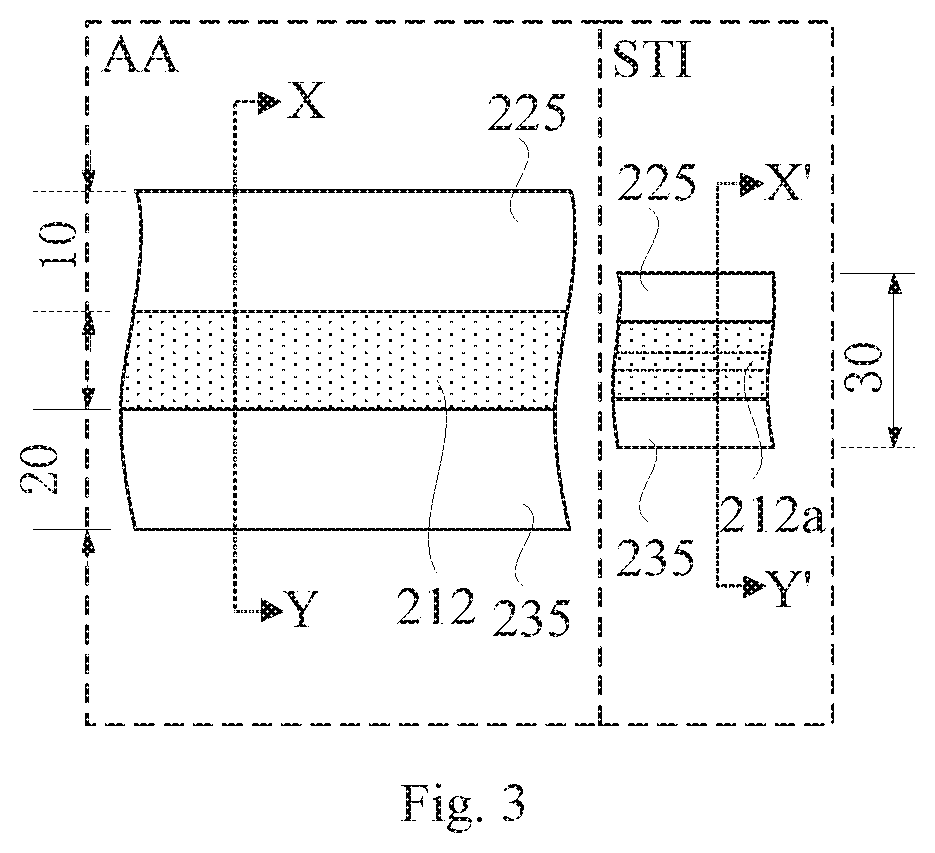
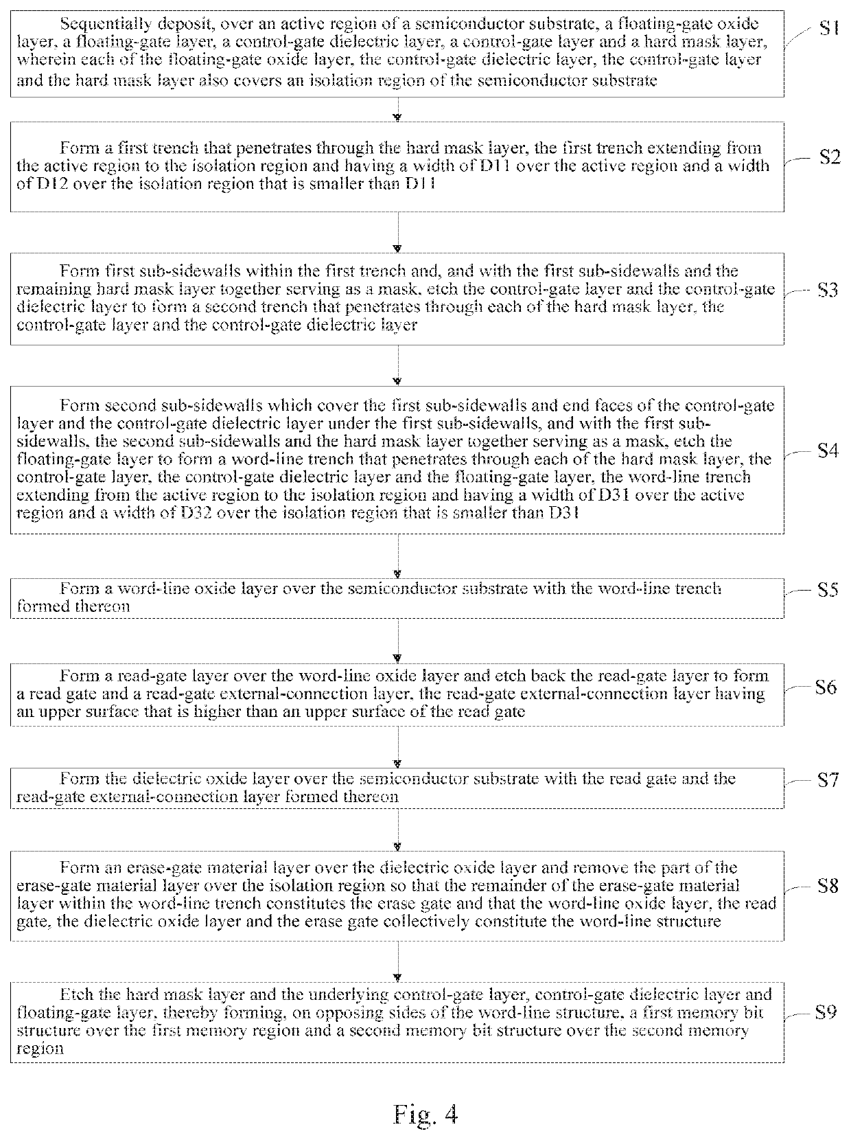
[0037]The split-gate flash memory, the method of fabricating the split-gate flash memory and the method for control thereof, proposed in the present invention will be described in greater detail with reference to a few specific embodiments which are to be read in conjunction with the accompanying drawings so that those skilled in the art can better understand the subject matter disclosed herein. Features and advantages of the invention will be more apparent from the following detailed description, and from the appended claims. Note that the accompanying drawings are provided in a very simplified form not necessarily presented to scale, with the only intention of facilitating convenience and clarity in explaining the several embodiments of the invention. Embodiments of the present invention should not be construed as being limited to the particular shapes illustrated in the appended figures. For the sake of clarity, like elements are principally given the same or analogous reference ...


PUM


Abstract

A split-gate flash memory, a method of fabricating the split-gate flash memory and a method for control thereof are disclosed. The split-gate flash memory includes: a semiconductor substrate including a first memory region and a second memory region that are separate from each other; and a word-line structure between the first memory region and the second memory region. The word-line structure includes, stacked on the surface of the semiconductor substrate sequentially from bottom to top, a word-line oxide layer, a read gate, a dielectric oxide layer and an erase gate. The read and erase gates can each function as a word line of the split-gate flash memory for enabling a read or erase operation. During the erase operation, a voltage applied on the erase gate has an insignificant impact on the underlying semiconductor substrate, which is helpful in reducing channel leakage in the semiconductor substrate.

Description

CROSS-REFERENCE TO RELATED APPLICATION[0001]This application claims the priority of Chinese patent application number 201810483313.5, filed on May 18, 2018, the entire contents of which are incorporated herein by reference.TECHNICAL FIELD[0002]The present invention relates to the field of semiconductor technology and, in particular, to a split-gate flash memory, a method of fabricating the split-gate flash memory and a method for control thereof.BACKGROUND[0003]Memory devices are used to store massive digital information. Over the past several years, advances in processes and techniques and market demands have given rise to increasing diversification of memory device species. Among the variety of existing memory devices, flash memories are developing particularly fast and have found extensive application because they can maintain the stored information for a long time without power supply, in addition to other many advantages including high integration, fast access, and ease of eras...

Claims


Application Information

Patent Timeline
Patent Type & Authority Applications(United States)
IPC IPC(8): H01L29/423H01L27/11521G11C16/04H01L29/788H01L29/66H01L21/28H01L21/3213G11C16/26G11C16/14
CPCH01L29/7883H01L29/66825G11C16/14H01L21/32139H01L29/40114G11C16/26G11C16/0408H01L27/11521H01L29/42328H10B41/30G11C16/0458G11C16/08H10B41/35
Inventor LIU, XIANZHOU
Owner SHANGHAI HUAHONG GRACE SEMICON MFG CORP
Why Eureka
Try Eureka