Valve component with multiple surface layers
a surface coating and valve technology, applied in the direction of valve operating means/release devices, natural mineral layered products, transportation and packaging, etc., can solve the problems of wear of the mating surface of the disk, easy to “lock up”, and become “sticky” , to achieve the effect of improving scratch and abrasion resistance, reducing the thickness of the amorphous diamond layer, and improving the hardness
- Summary
- Abstract
- Description
- Claims
- Application Information
AI Technical Summary
Benefits of technology
Problems solved by technology
Method used
Image
Examples
example 1
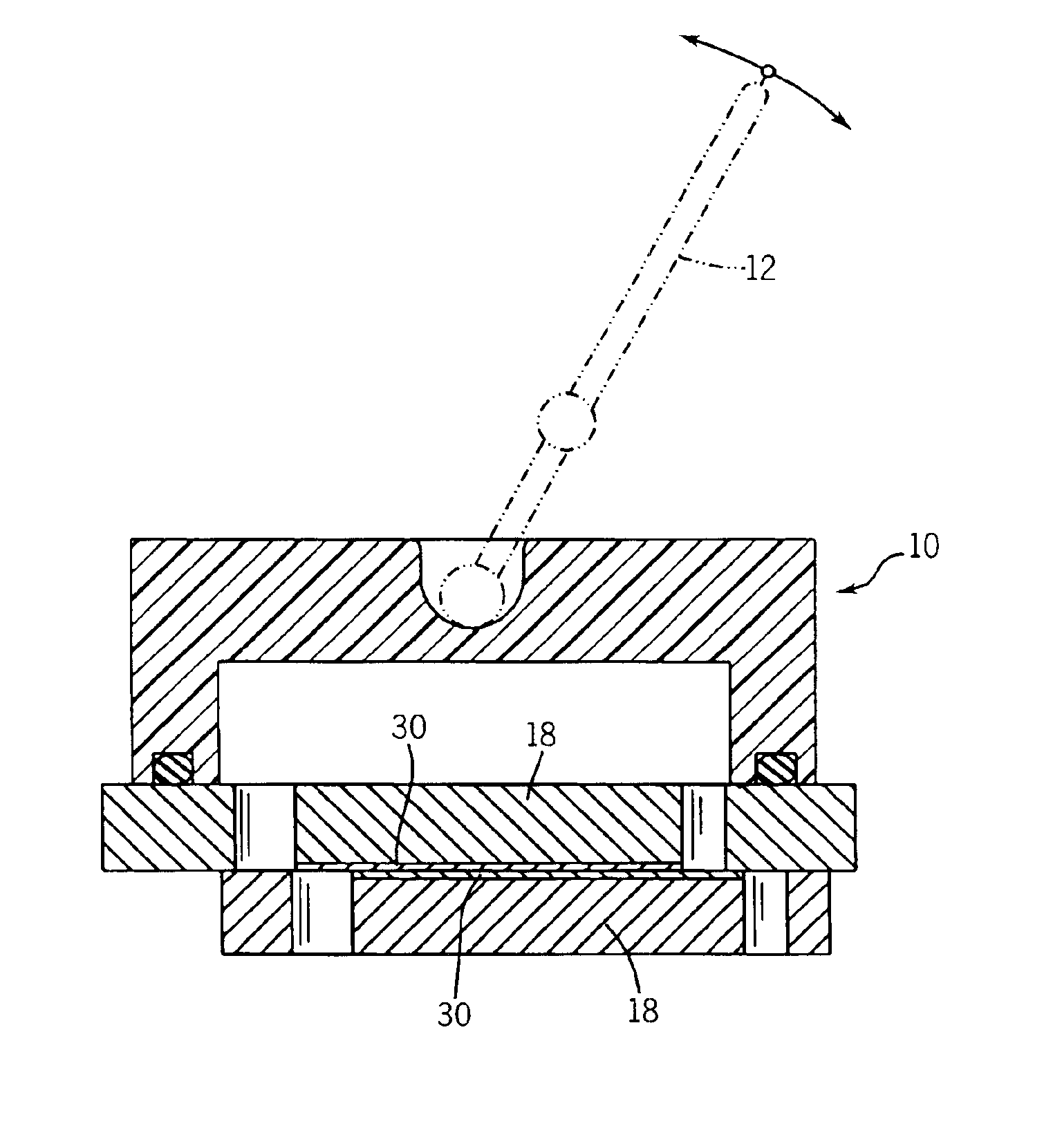
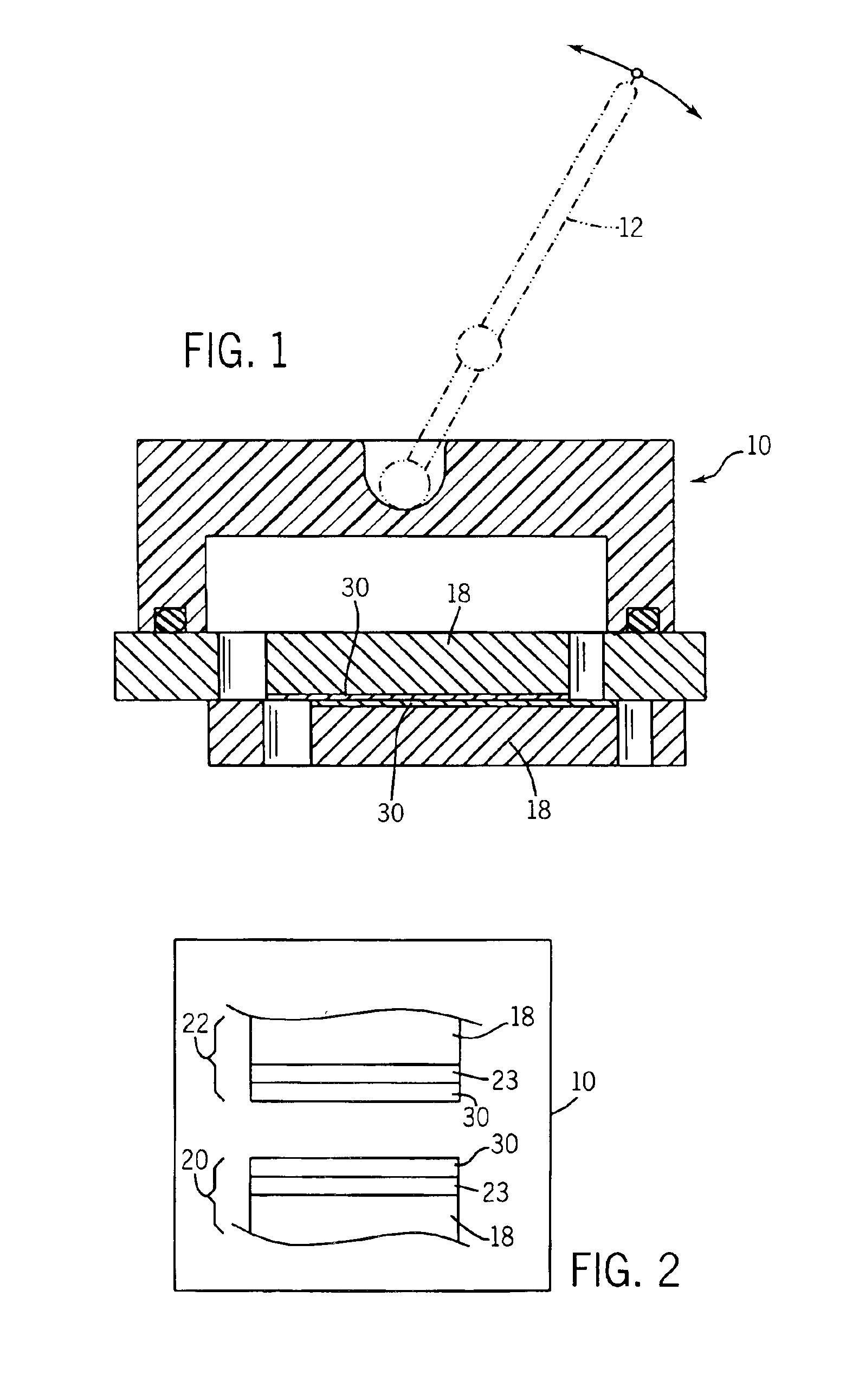
[0033]Clean stainless steel valve disks are placed in a vacuum deposition chamber incorporating an arc evaporation cathode and a sputtering cathode. The arc source is fitted with filtering means to reduce macroparticle incorporation in the coating, as described for example in U.S. Pat. Nos. 5,480,527 and 5,840,163, incorporated herein by reference. Sources of argon and nitrogen are connected to the chamber through a manifold with adjustable valves for controlling the flowrate of each gas into the chamber. The sputtering cathode is connected to the negative output of a DC power supply. The positive side of the power supply is connected to the chamber wall. The cathode material is chromium. The valve disks are disposed in front of the cathode, and may be rotated or otherwise moved during deposition to ensure uniform coating thickness. The disks are electrically isolated from the chamber and are connected through their mounting rack to the negative output of a power supply so that a bi...
example 2
[0038]Clean zirconium valve disks are placed into an air oven, heated to a temperature of 560 C., held at this temperature for about 6 hours, and cooled. A strengthening layer of zirconium oxide is thereby formed on the substrate surface, having a thickness of 5-10 microns. The disks are then placed in a vacuum deposition chamber incorporating a filtered arc evaporation cathode and a sputtering cathode. An adhesion layer of chromium having a thickness of about 20 nm is deposited on the valve disks by sputtering as described in example 1. After the chromium adhesion layer is deposited, an amorphous diamond layer is deposited as described in Example 1.
[0039]Valve disks made of zirconium and treated as described to form a multilayer structure on their surfaces were tested for scratch resistance, using a scratch tester with variable loading. The scratch depths generated on the treated Zr disks by a stylus tip having 100 micron radius under a load of 3 Newtons were around 4.7 microns dee...
example 3
[0040]Clean molded-glass valve disks are placed in a vacuum deposition chamber incorporating a laser ablation source, a PECVD source, and a sputtering cathode. The valve disks are subjected to a RF (radio-frequency) discharge plasma cleaning by known means. An adhesion layer of titanium having a thickness of about 20 nm is then deposited on the valve disks by sputtering. A strengthening layer of DLC having thickness of about 3 microns is then deposited on top of the adhesion layer by PECVD using known deposition parameters. An amorphous diamond layer having thickness of about 300 nm is then deposited on top of the DLC layer by laser ablation using typical deposition parameters.
PUM
| Property | Measurement | Unit |
|---|---|---|
| temperature | aaaaa | aaaaa |
| thickness | aaaaa | aaaaa |
| thickness | aaaaa | aaaaa |
Abstract
Description
Claims
Application Information


