Semiconductor processing techniques utilizing vacuum ultraviolet reflectometer

a technology of ultraviolet reflectometer and semiconductor, applied in the direction of instruments, spectrometry/spectrophotometry/monochromators, optical radiation measurement, etc., can solve the problems of reduced sensitivity of semiconductor instruments to changes in processing conditions, inability of semiconductor manufactures to adequately control process equipment, and limitations of conventional optical instruments, so as to achieve heightened sensitivity to small changes in processing conditions

Active Publication Date: 2006-04-11
BRUKER TECH LTD
View PDF35 Cites 37 Cited by
  • Summary
  • Abstract
  • Description
  • Claims
  • Application Information

AI Technical Summary

Benefits of technology

[0015]An objective of the current invention is to provide the semiconductor manufacturing industry with a reliable optical metrology tool that is capable of characterizing semiconductor devices incorporating thinner layers and smaller features. This instrument will take full advantage of the heightened levels of sensitivity to small changes in processing conditions that are afforded through the characterization of materials at and below the VUV wavelength region. This instrument will be non-contact and non-destructive and will make use of referenced reflectometry data.
[0016]The design of the instrument is simple and robust rendering it easy to operate at VUV wavelengths. As a result of its simplicity it is fast, thereby lending it to use in high throughput manufacturing applications. The system is designed such that it is compact and requires little space. The instrument offers the advantage of minimizing environmental effects so far as to remove the need to sustain a reproducible controlled environment during the course of calibration, referencing and sample measurement. Additionally, it offers a small measurement spot size such that in-line measurements on product samples are possible and employ imaging optics such that multiple measurements on a series of sites within a localized region can be obtained simultaneously.
[0018]In another embodiment, a spectroscopy system is provided which operates in the vacuum ultra-violet spectrum. More particularly, a system utilizing reflectometry techniques in the vacuum ultraviolet spectrum is provided for use in metrology applications. To ensure accurate and repeatable measurement, the environment of the optical path is controlled to limit absorption effects of gases that may be present in the optical path. To account for absorption effects that may still occur, the length of the optical path is minimized. To further account for absorption effects, the reflectance data may be referenced to a relative standard. Referencing is particularly advantageous in the VUV reflectometer due to the low available photon flux and the sensitivity of recorded data to the composition of the gaseous medium contained with the optical path. Thus, errors that may be introduced by changes in the controlled environment may be reduced. In one exemplary embodiment, the VUV reflectometer may utilize a technique in which a beam splitter is utilized to create a sample beam and a reference beam to form the two arms of a near balanced Mach Zehnder interferometer. In another exemplary embodiment, the reference channel may be comprised of a Michelson interferometer.

Problems solved by technology

Unfortunately, as semiconductor processing technologies progress, and as device geometries shrink, the sensitivity of such instruments to changes in processing conditions is reduced.
Without sensitive, accurate, and repeatable feedback from metrology instrumentation, semiconductor manufactures are unable to adequately control process equipment and hence, achieve high yields.
In short, conventional optical instrumentation is reaching limitations that make it unsuitable for future technologies.
All of these companies, however, have designed instruments that rely on ellipsometric techniques, which by their very nature require complicated hardware and control systems.
Such devices are typically slow and not capable of sustaining the high level measurement throughput required in semiconductor manufacturing environments.
In addition, such instruments generally employ numerous transmissive polarizing elements which effectively limit the shortest wavelength photons that can be employed.
As a result, current VUV ellipsometric metrology systems can only operate at wavelengths longer than about 140 nm.
While this approach does attempt to make use of the improved signal distinguishing ability imparted by the use of higher energy photons, it also suffers from the aforementioned complications associated with the employment of complicated ellipsometric techniques.
If the conditions change, instrument repeatability and stability will be adversely affected.
Reproducible steady-state conditions would be difficult to achieve using such an arrangement as flow characteristics could be expected to change considerably depending on the placement of the sample during measurement.
As such, these systems are time consuming and not well-suited to the needs of semiconductor manufacturers.
Numerous referencing techniques exist in the prior art, generally however these methods are either time consuming, and involve mechanically positioning a reference sample into and out of the sample location, or employ separate detection components (i.e. diffraction elements and detectors) for sample and reference measurements which can lead to inaccurate results.
The approach is time-consuming since it requires scanning of the dispersion grating and also suffers from the detector issues described earlier.

Method used


Image

  • Semiconductor processing techniques utilizing vacuum ultraviolet reflectometer
  • Semiconductor processing techniques utilizing vacuum ultraviolet reflectometer
  • Semiconductor processing techniques utilizing vacuum ultraviolet reflectometer

Examples


Embodiment Construction

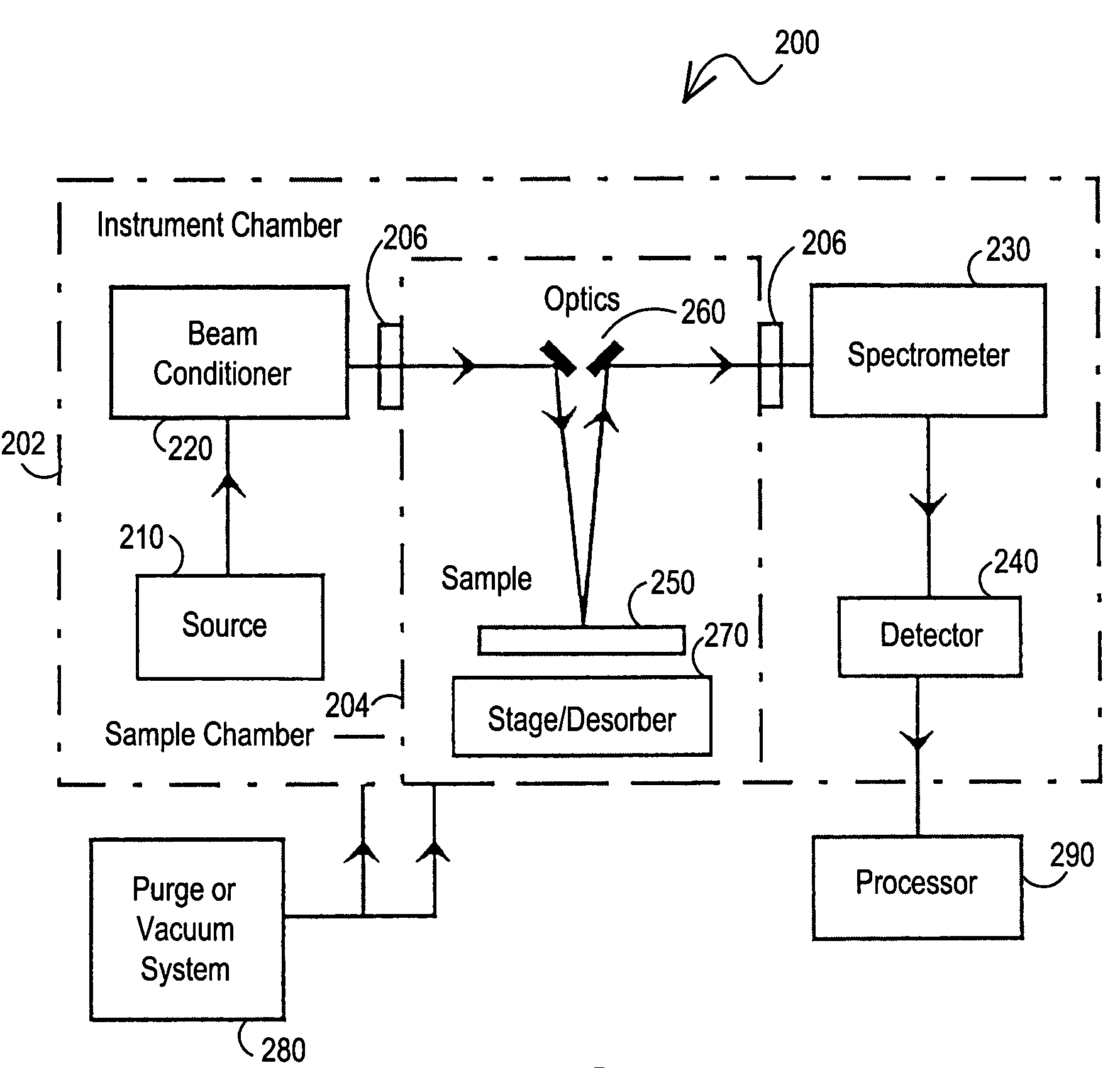
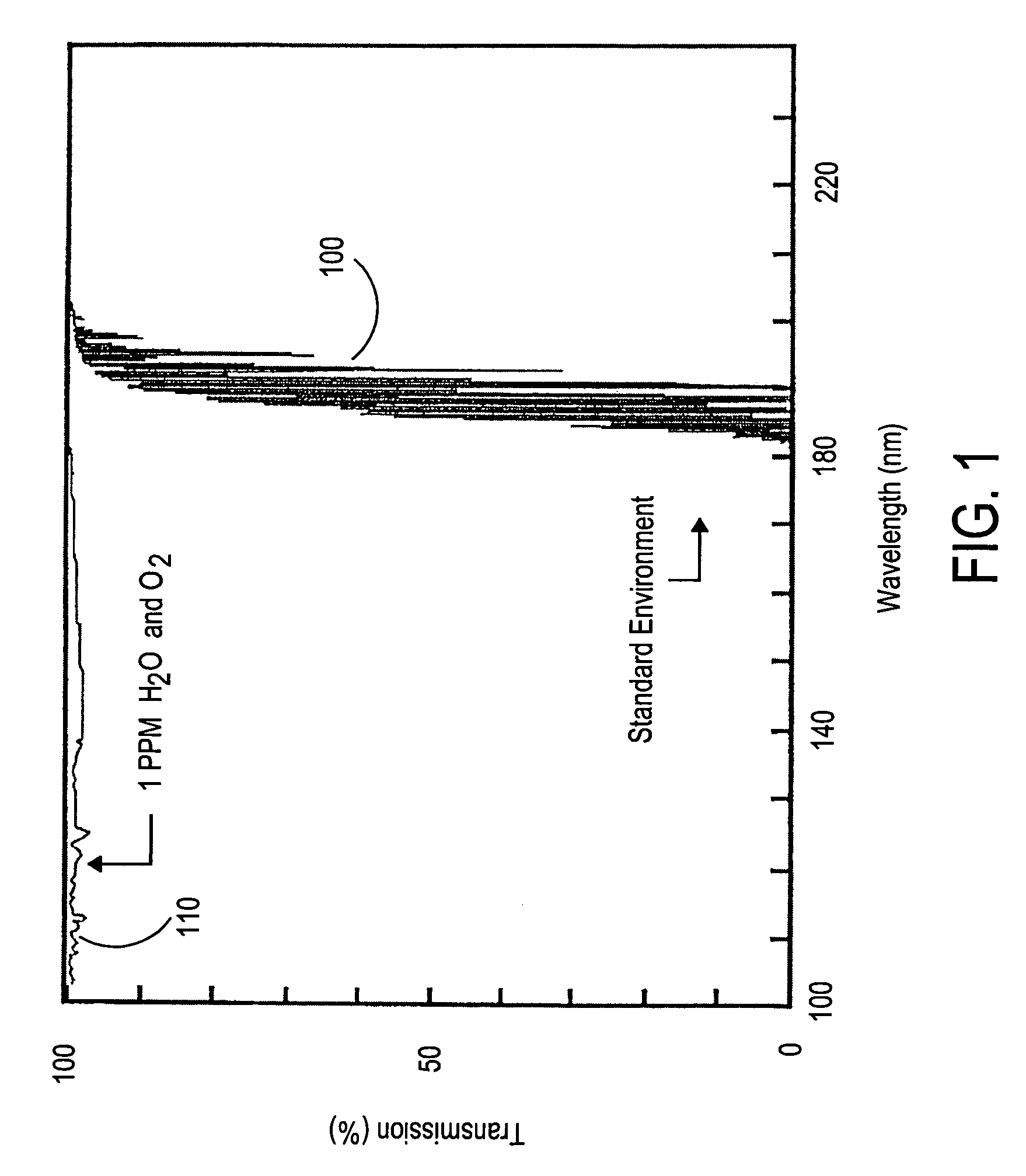
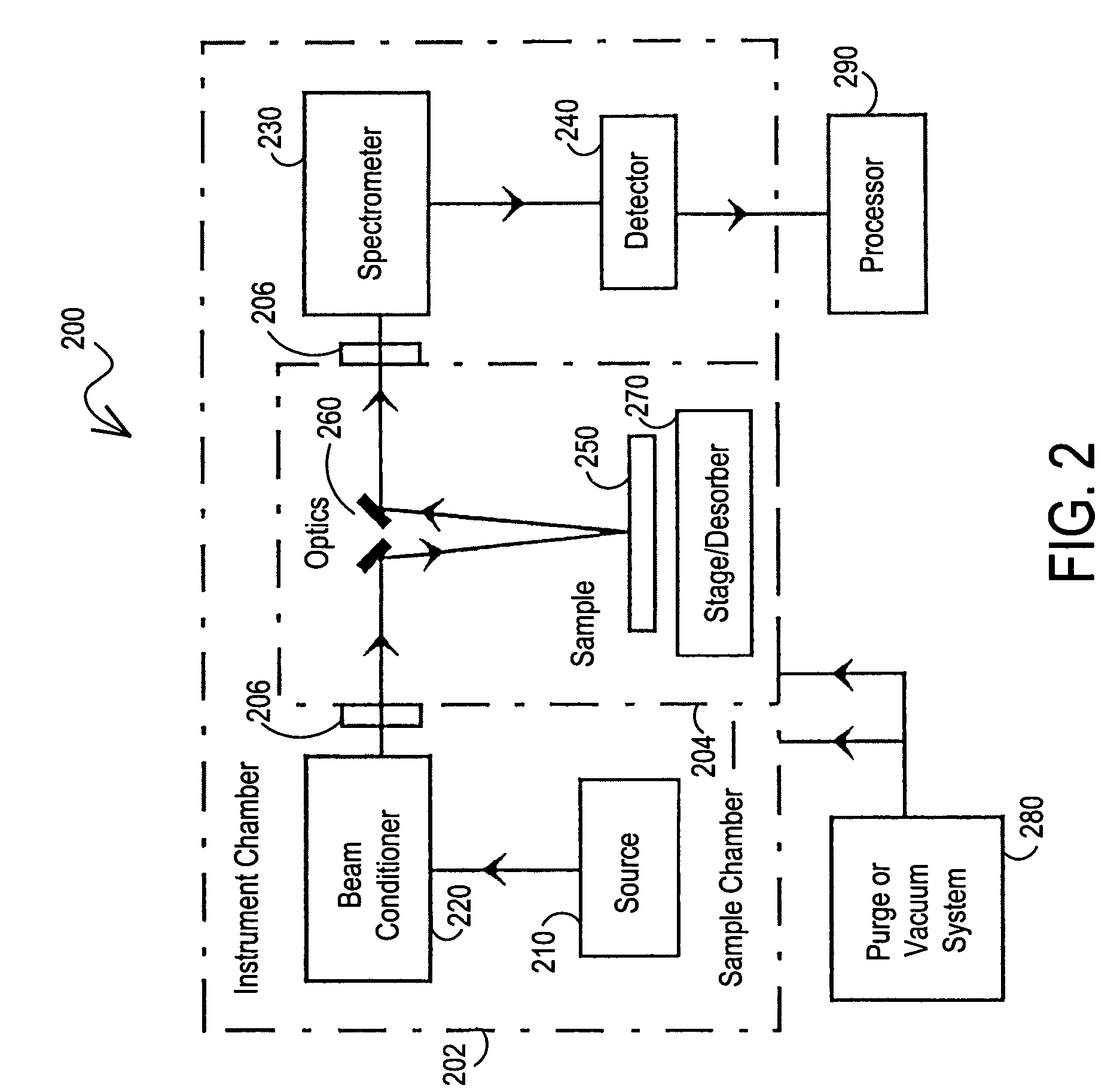
[0056]To enhance the sensitivity of optical metrology equipment for challenging applications it is desirable to extend the range of wavelengths over which such measurements are performed. Specifically, it is advantageous to utilize shorter wavelength (higher energy) photons extending into, and beyond, the region of the electromagnetic spectrum referred to as the vacuum ultra-violet (VUV). Historically there has been relatively little effort expended on the development of optical instrumentation designed to operate at these wavelengths, owing to the fact that VUV (and lower) photons are strongly absorbed in standard atmospheric conditions. Vacuum ultra-violet (VUV) wavelengths are generally considered to be wavelengths less than deep ultra-violet (DUV) wavelengths. Thus VUV wavelengths are generally considered to be wavelengths less than about 190 nm. While there is no universal cutoff for the bottom end of the VUV range, some in the field may consider VUV to terminate and an extreme...


PUM

PropertyMeasurementUnit
wavelengthsaaaaaaaaaa

Abstract

A spectroscopy system is provided which operates in the vacuum ultraviolet spectrum. More particularly, a system utilizing reflectometry techniques in the vacuum ultraviolet spectrum is provided for use in metrology applications. To ensure accurate and repeatable measurement, the environment of the optical path is controlled to limit absorption effects of gases that may be present in the optical path. The VUV reflectometer may be utilized to monitor a wide range of data in a semiconductor processing environment. For example, the techniques may be used for measuring thicknesses, optical properties, composition, porosity and roughness of a film or stack of films. Further, the VUV techniques and apparatus may be used to characterize critical dimensions and other features of a device. The VUV reflectometer system may be utilized as a stand alone tool, or the relatively compact nature of the system may be taken advantage of such that the system is incorporated into other process tools. Thus, for example, the VUV techniques described herein may be incorporated directly into tools used for deposition, etch, photolithography, etc. so that in-line measurements, monitoring and control may be advantageously obtained.

Description

CROSS-REFERENCE TO RELATED APPLICATIONS[0001]This application claims priority to U.S. provisional patent Ser. Nos. 60 / 440,434 filed Jan. 16, 2003, 60 / 440,435 filed Jan. 16, 2003, and 60 / 440,443 filed Jan. 16, 2003, the disclosures of which are each expressly incorporated herein by reference. This application also expressly incorporates by reference concurrently filed U.S. patent application Ser. No. 10 / 668,642, entitled “Vacuum Ultraviolet Reflectometer System and Method” by Dale A. Harrison, and concurrently filed U.S. patent application Ser. No. 10 / 668,644, entitled “Vacuum Ultraviolet Referencing Reflectometer” by Dale A. Harrison.BACKGROUND OF THE INVENTION[0002]The present invention relates generally to instrumentation for, and applications of, vacuum ultraviolet reflectance spectroscopy. In one embodiment, the invention can be used to provide semiconductor manufacturers with high throughput, non-contact metrology capabilities for use in process control during the manufacturing...

Claims


Application Information

Patent Timeline
Patent Type & Authority Patents(United States)
IPC IPC(8): G01N21/33G01J3/28G01J3/36G01N21/21G01N21/47G01N21/55
CPCG01J3/2803G01J3/2823G01N21/55G01N21/33G01J3/36G01J3/021G01J3/0286G01N21/211G01N21/47
Inventor HARRISON, DALE A.
Owner BRUKER TECH LTD
Why Eureka
Try Eureka