Semiconductor variable capacitor

A technology of variable capacitors and semiconductors, applied in semiconductor devices, circuits, electrical components, etc., can solve the problems of limiting the frequency modulation range of semiconductor variable capacitors, reducing the quality factor Q performance of semiconductor variable capacitors, etc., to increase width and improve frequency modulation range effect

Inactive Publication Date: 2010-09-15
SEMICON MFG INT (SHANGHAI) CORP
View PDF0 Cites 6 Cited by
  • Summary
  • Abstract
  • Description
  • Claims
  • Application Information

AI Technical Summary

Problems solved by technology

[0012] For semiconductor variable capacitors using CMOS process technology, due to the existence of LDD/Pck, the frequency modulation range of

Method used


Image

  • Semiconductor variable capacitor
  • Semiconductor variable capacitor
  • Semiconductor variable capacitor

Examples


Embodiment 1

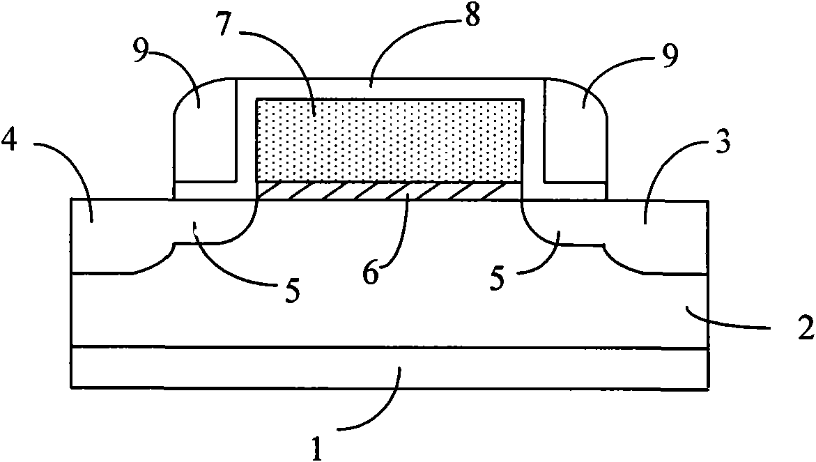
[0060] For the semiconductor variable capacitor provided in the first embodiment, please refer to figure 2 , the semiconductor variable capacitor consists of:

[0061] A semiconductor substrate 1, the semiconductor substrate can be formed by using a P-type substrate.

[0062] The N-type ion trap 2 is located on the semiconductor substrate 1, and a plurality of ion-doped regions are arranged in it, and each region is used as a source 3 or a drain 4 respectively.

[0063] The gate dielectric layer 6 is located on the ion trap 2, and the gate dielectric layer 6 is a nitride or an oxide, such as silicon nitride or silicon dioxide.

[0064] The gate 7 is located between the source 3 and the drain 4 and superimposed on the gate dielectric layer 6. The gate 7 is a polysilicon gate or a metal gate. In this embodiment, N-type polysilicon is selected. as gate 7.

[0065] The insulating layer 8 is located on the upper surface of the N-type ion trap 2 , the sidewall formed by stacking...

Embodiment 2

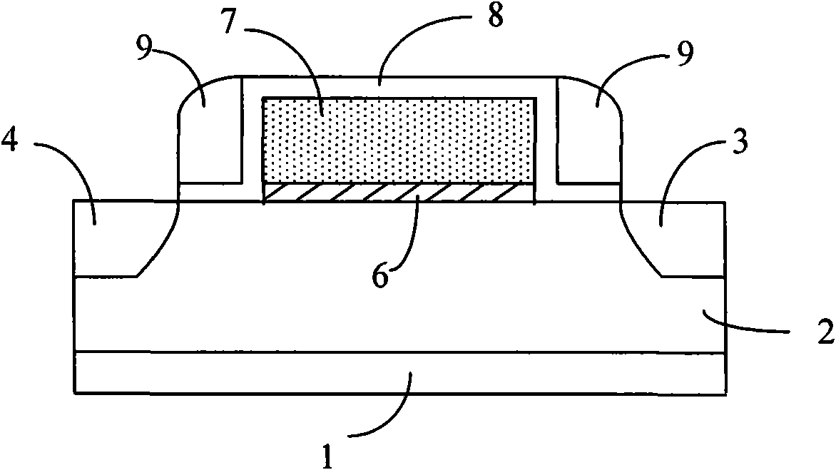
[0073] see figure 2 , the semiconductor variable capacitor consists of:

[0074] A semiconductor substrate 1, the semiconductor substrate can be formed by using a P-type substrate.

[0075] The P-type ion trap 2 is located on the semiconductor substrate 1, and a plurality of ion-doped regions are arranged in it, and each region is used as a source 3 or a drain 4 respectively.

[0076] The gate dielectric layer 6 is located on the P-type ion trap 2, and the gate dielectric layer 6 is a nitride or an oxide, such as silicon nitride or silicon dioxide.

[0077] The gate 7 is located between the source 3 and the drain 4 and superimposed on the gate dielectric layer 6. The gate 7 is a polysilicon gate or a metal gate. In this embodiment, P-type polysilicon is selected. as gate 7.

[0078] The insulating layer 8 is located on the upper surface of the P-type ion trap 2 , the sidewall formed by stacking the gate dielectric layer 6 and the P-type polysilicon gate 7 , and the upper s...

Embodiment 3

[0082] see figure 2 , the semiconductor variable capacitor consists of:

[0083] A semiconductor substrate 1, the semiconductor substrate can be formed by using a P-type substrate.

[0084] The P-type ion trap 2 is located on the semiconductor substrate 1, and a plurality of ion-doped regions are arranged in it, and each region is used as a source 3 or a drain 4 respectively.

[0085] The gate dielectric layer 6 is located on the P-type ion trap 2, and the gate dielectric layer 6 is a nitride or an oxide, such as silicon nitride or silicon dioxide.

[0086] The gate 7 is located between the source 3 and the drain 4 and superimposed on the gate dielectric layer 6. The gate 7 is a polysilicon gate or a metal gate. In this embodiment, N-type polysilicon is selected. as gate 7.

[0087] The insulating layer 8 is located on the upper surface of the P-type ion trap 2 , the sidewall formed by stacking the gate dielectric layer 6 and the N-type polysilicon gate 7 , and the upper s...


PUM


Abstract

The invention provides a semiconductor variable capacitor which comprises a semiconductor substrate, an ion trap, a gate dielectric layer, a gate and an insulation layer, wherein the ion trap is arranged on the semiconductor substrate, a plurality of ion doping areas are arranged in the ion trap, and each area is respectively used as a source or a drain; the gate dielectric layer is arranged on the ion trap; the gate is arranged between the source and the drain and is stacked on the gate dielectric layer; the insulation layers are arranged on the upper surface of the ion trap, the side wall stacked by the gate dielectric layer and the gate, and the upper surface of the gate and the sides of the insulation layers are provided with side walls. Compared with the traditional semiconductor variable capacitor, as the semiconductor variable capacitor is arranged on the overlapping part of the gate and the drain, and the overlapping part of the gate and the source, the doping concentration ratio of the invention is lighter than that of the semiconductor variable capacitor containing LDD/Pck, the width of the consumed layer is increased, the capacitor Cf values between the gate and the source and between the gate and the drain are decreased, and thus, the frequency modulating range of the capacitor is enhanced.

Description

technical field [0001] The invention relates to a variable capacitor, in particular to a semiconductor variable capacitor. Background technique [0002] Semiconductor variable capacitance element (Varactor) is one of the key components in the field of electronic technology, and can be widely used in integrated circuit systems such as digital, analog, digital-analog hybrid, and radio frequency. In digital or analog systems, such as ADC / DAC (analog-to-digital conversion / digital-to-analog conversion) or high-speed communication systems, designers pay more attention to the frequency modulation range and device measurability of capacitors; for RF applications, designers must consider the capacitance of capacitors FM range, but also consider improving Q (quality factor) to improve anti-interference performance. [0003] Now that the semiconductor process has entered the deep submicron process, with the further reduction of the feature size of the semiconductor device, the high el...

Claims


Application Information

Patent Timeline
IPC IPC(8): H01L29/94H01L29/36
Inventor 程仁豪
Owner SEMICON MFG INT (SHANGHAI) CORP
Why Eureka
Try Eureka