Silicon carbide power device and preparation method thereof

A technology of power devices and silicon carbide, which is applied in semiconductor/solid-state device manufacturing, semiconductor devices, electrical components, etc., can solve the problems of low device channel mobility and large on-resistance, and achieve improved channel mobility and channel The effect of track density

Pending Publication Date: 2022-04-05
PEKING UNIV
View PDF0 Cites 6 Cited by
  • Summary
  • Abstract
  • Description
  • Claims
  • Application Information

AI Technical Summary

Problems solved by technology

[0014] The purpose of the present invention is to propose a silicon carbide power MOSFET structure to solve the problems of low device channel mobility and large on-resistance

Method used


Image

  • Silicon carbide power device and preparation method thereof
  • Silicon carbide power device and preparation method thereof
  • Silicon carbide power device and preparation method thereof

Examples


Embodiment 1

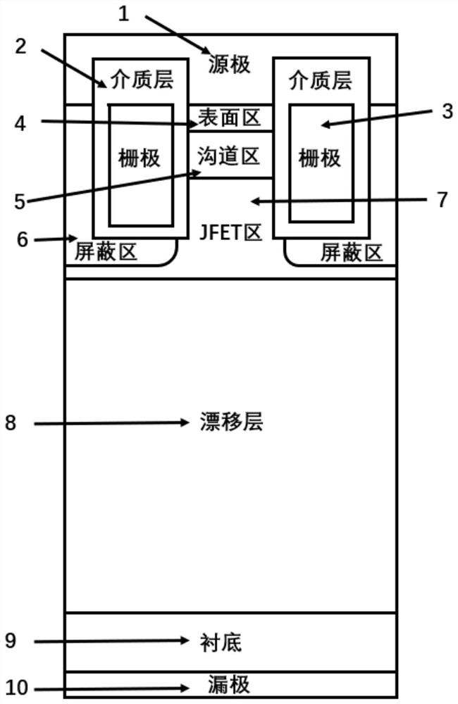
[0057] The structure of the SiC power device prepared in this embodiment is as follows figure 1 As shown, it includes the substrate 9 required for epitaxy (in order to form ohmic contact with the electrode, it needs to be heavily doped), the drift layer 8 as a withstand voltage structure, the shielding region 6 for shielding the high electric field at the bottom of the gate dielectric layer, and the middle of the shielding region 6 Appropriately doped to reduce the JFET region 7 of the on-resistance, the surface in contact with the gate 3 produces the channel region 5 of the channel inversion layer when the device is turned on, and the heavy doping between the channel region 5 and the electrode (for the same purpose Ohmic contact) surface region 4, contact electrodes such as gate 3, drain 10, source 1, etc., gate dielectric layer 2 around gate 3, and passivation layer, field plate, etc. necessary in traditional SiC power devices Although the structures are not shown in the fig...

Embodiment 2

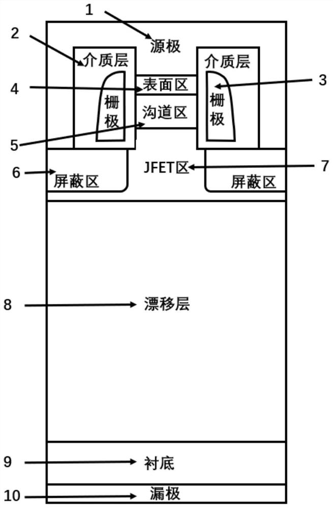
[0071] The structure of the SiC power device prepared in this embodiment is as follows figure 2 shown, with figure 1 The difference of the structure shown is that the shielding region 6 is changed from surrounding the gate 3 to being at the bottom of the gate 3 .

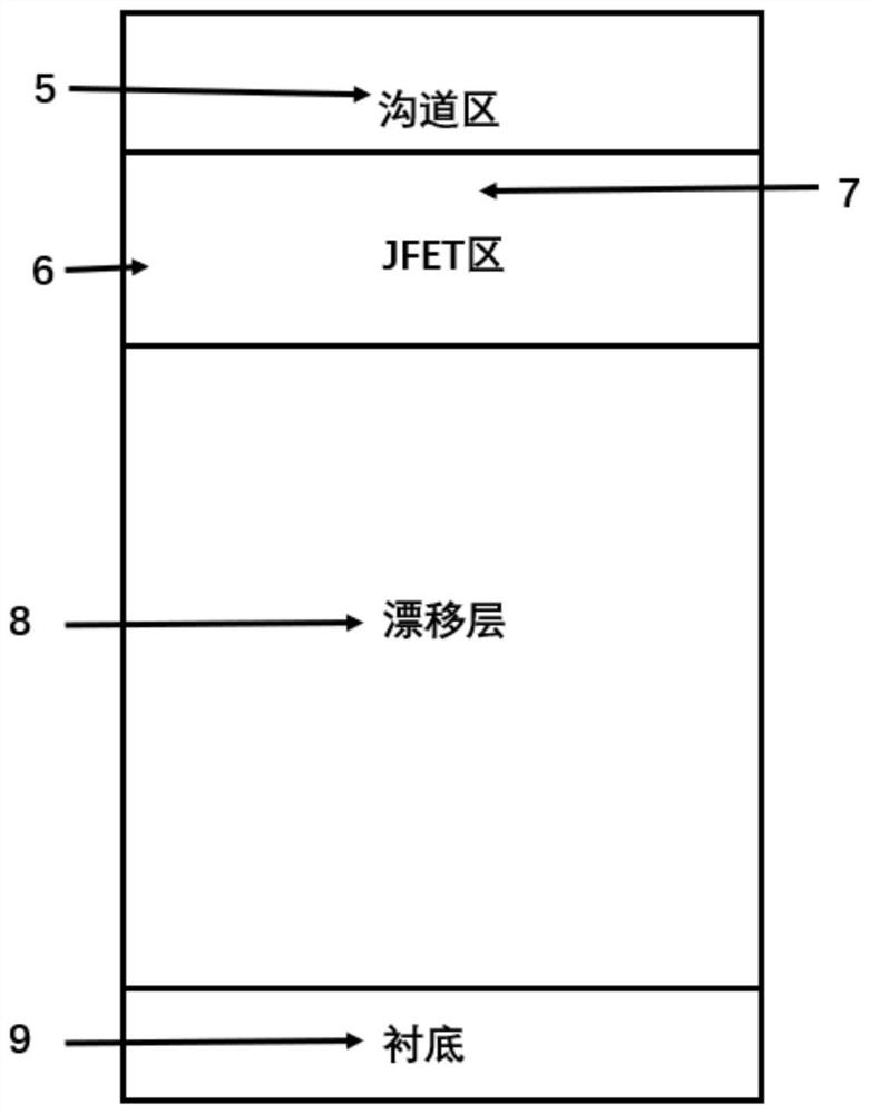
[0072] Step 1. First select N + type silicon carbide substrate 9, on which epitaxially grow N - Type drift layer 8, N-type JFET region 7, channel region 5 and surface region 4, such as Figure 8 shown;

[0073] The thickness is selected as 350 μm, and the doping concentration of phosphorus ions is 5×10 19 cm -3 N + Type SiC substrate 9, cleaned, vapor phase epitaxial growth thickness of 10 μm, phosphorus ion doping concentration of 8×10 15 cm -3 N - The drift layer 8 has a thickness of 3 μm and a phosphorus ion doping concentration of 3×1016 cm -3 The N-type JFET region 7 has a thickness of 0.5 μm and an aluminum ion doping concentration of 1E16cm -3 (or 8E15cm -3 ) of the channel region 5 (so that the ...


PUM

PropertyMeasurementUnit
thicknessaaaaaaaaaa
thicknessaaaaaaaaaa
thicknessaaaaaaaaaa

Abstract

The invention discloses a silicon carbide power device and a preparation method thereof. The device is a silicon carbide MOSFET of a longitudinal structure and comprises a drain electrode, an N + type silicon carbide substrate, an N-type drift layer, an N type JFET region and a channel region which are sequentially arranged from bottom to top, the N type JFET region and the channel region form a fin-type structure, and the two sides of the N type JFET region and the channel region are each provided with a gate structure; a P-type shielding region is arranged at the bottom of the gate structure, or the P-type shielding region surrounds the bottom of the gate structure and is far away from the outer side of the fin-type structure; an N + type surface region is arranged on the channel region, and a source electrode in ohmic contact with the N + type surface region and the surface of a part of the P type shielding region is arranged on the N + type surface region; and the drain electrode is in ohmic contact with the lower surface of the N + type silicon carbide substrate. According to the silicon carbide power device, the well grounded P-type shielding region is manufactured to shield the gate dielectric layer, and meanwhile, the low-doped depletion channel region which does not need to be grounded is introduced, so that the channel mobility and the channel density are further improved, and the on resistance of the device is reduced.

Description

technical field [0001] The invention provides a silicon carbide power device, in particular to a trench gate silicon carbide power MOSFET (Metal-Oxide-Semiconductor Field-Effect Transistor, metal oxide semiconductor field-effect transistor), which belongs to the field of power electronic devices. Background technique [0002] Power devices refer to semiconductor devices that can handle high voltage and high current, and are often used in electric energy change and control circuits. Silicon carbide is a representative material in wide bandgap semiconductors. It has many advantages such as high critical breakdown electric field, high thermal conductivity and high electron saturation drift rate, and is widely used in the field of power electronics. [0003] Silicon carbide power MOSFET is a power device made of the excellent performance of silicon carbide, and it is a promising method to further improve the performance of power switching systems. According to the structure of ...

Claims


Application Information

Patent Timeline
Patent Type & Authority Applications(China)
IPC IPC(8): H01L29/78H01L21/336H01L29/16H01L29/167H01L29/423
Inventor 魏进崔家玮杨俊杰
Owner PEKING UNIV
Why Eureka
Try Eureka