Method for electrically and mechanically connecting microstructures using solder

a microstructure and electrical connection technology, applied in semiconductor/solid-state device testing/measurement, semiconductor/solid-state device details, instruments, etc., can solve the problems of insufficient size of the board, insufficient electrical connection, and insufficient electrical connection

Inactive Publication Date: 2005-05-17
RGT UNIV OF MICHIGAN
View PDF5 Cites 45 Cited by
  • Summary
  • Abstract
  • Description
  • Claims
  • Application Information

AI Technical Summary

Benefits of technology

[0022]Further in carrying out the above object and other objects of the present invention, a method for locally connecting a plurality of microstructures is provided. The method includes the step of aligning the microstructures to form aligned pairs of microstructures. The microstructures of each aligned pa...

Problems solved by technology

For instance, a biologist may need to swap damaged off-board sensors in an insect-mounted microsystem without removing the system and returning to the laboratory.
Although this system 10 is sufficient for use with some insects, its size is prohibitively large for many others.
The connectors 16 around the perimeter of the platform shown in FIG. 1 enable sensors to be connected and di...

Method used


Image

  • Method for electrically and mechanically connecting microstructures using solder
  • Method for electrically and mechanically connecting microstructures using solder
  • Method for electrically and mechanically connecting microstructures using solder

Examples


Embodiment Construction

)

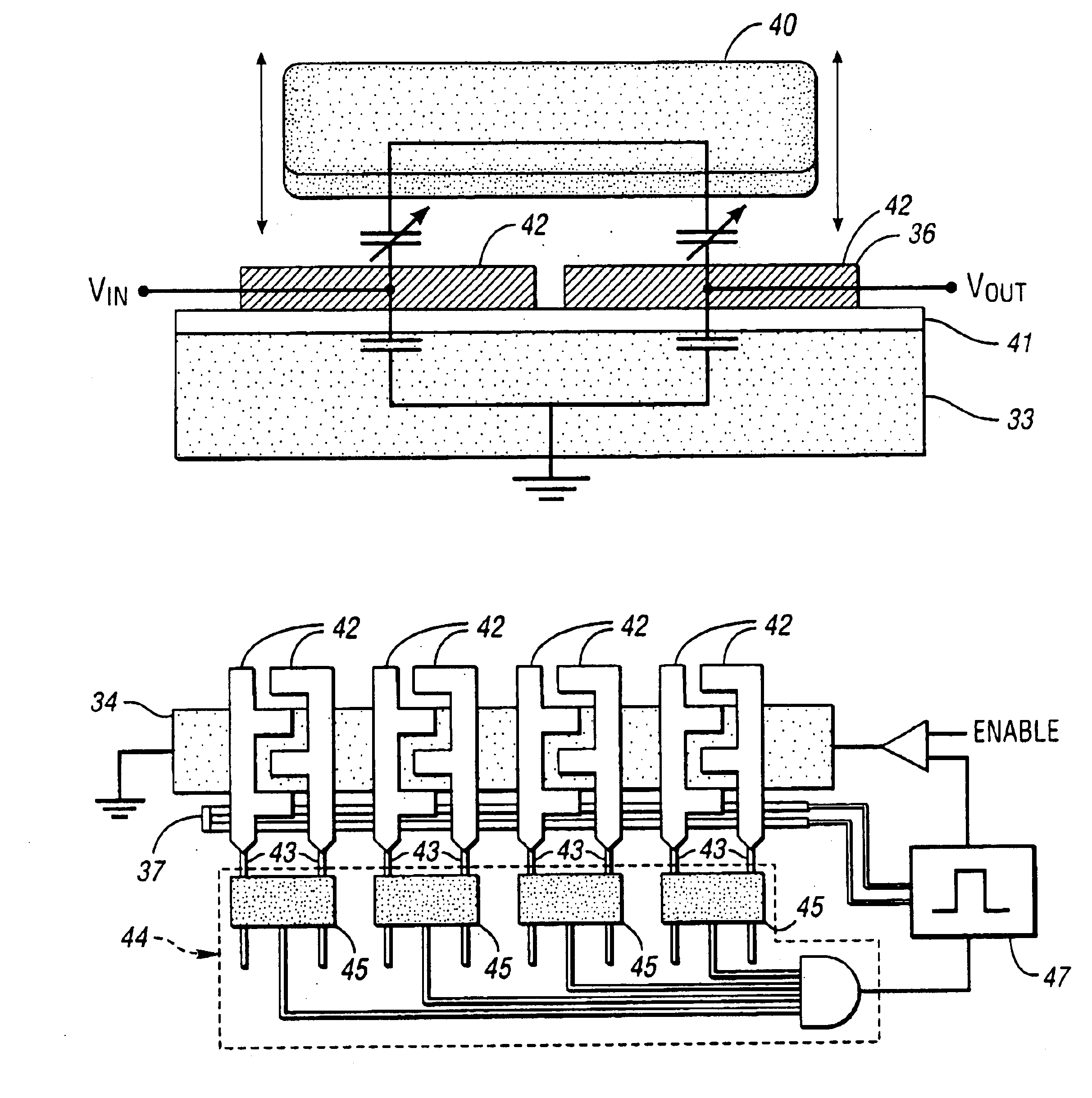
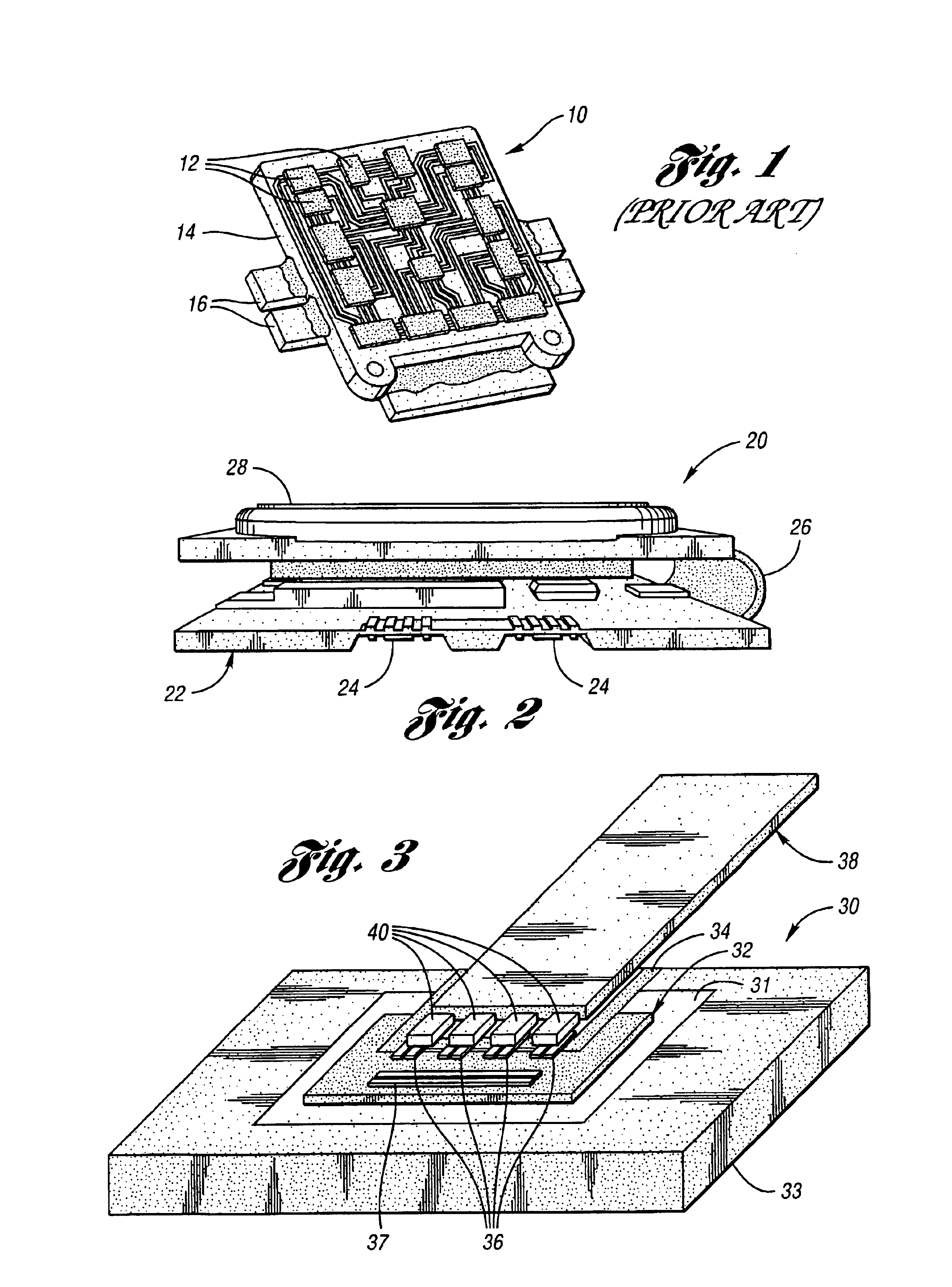
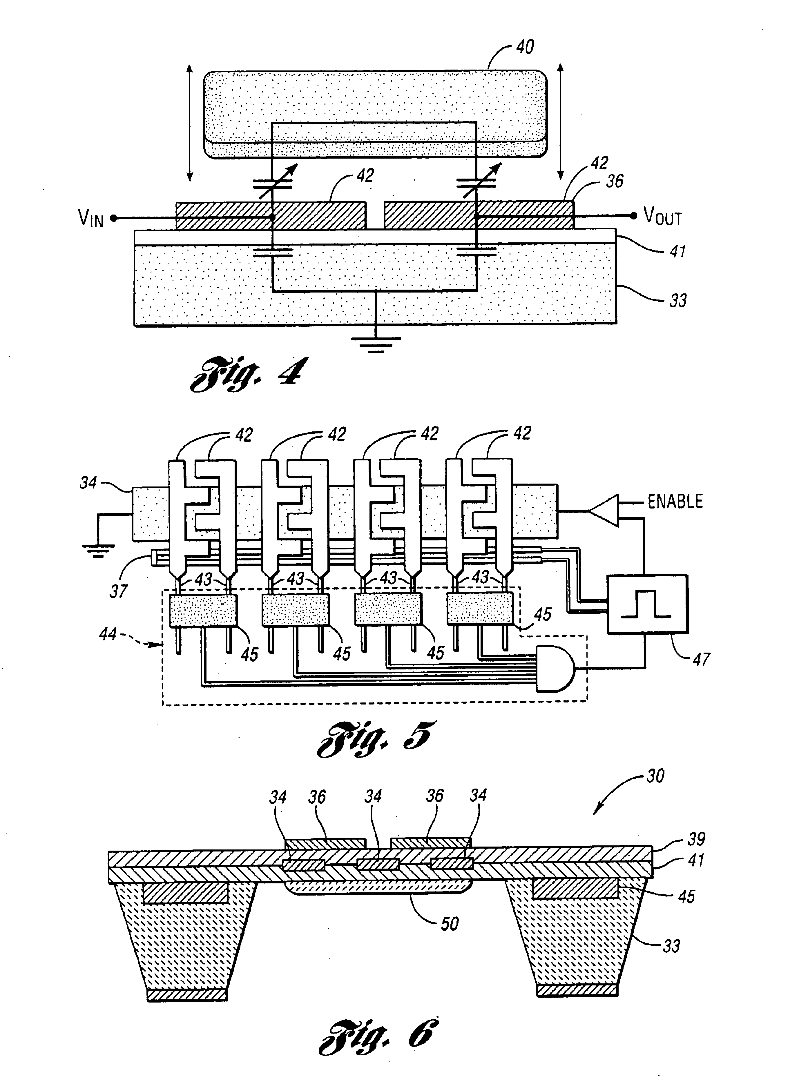
[0050]In general, solder-based microconnections in which contact is automatically detected in the bonding pad area to initiate bonding by triggering localized heating of solder is described herein. This approach requires very little force and no equipment beyond a positioning tool or manipulator. FIG. 2 illustrates a system, generally indicated at 20, that implements such microconnections along with some of the aforementioned approaches to shrinking the size of Microsystems. The system 20 includes a CMOS multi-chip module 22, solder-based microconnections 24, a folding hinge assembly 26 and a battery or power source 28.

[0051]For the microconnections, heat is applied directly under metal contact pads on a silicon substrate. When a device with pre-soldered lead tabs contacts the heated pads, the solder melts and establishes the desired bonds between the lead tabs and the pads. By confining the heated region to a very small area using thermal isolation, relatively low power is consume...


PUM


Abstract

A method and system for locally connecting microstructures and devices formed thereby are provided wherein localized solder-bonding creates bonds between pairs of microstructures found on miniature flexible cables and silicon microsystem platforms. Multi-lead contact to the pads are detected automatically, triggering an embedded heater or heaters to initiate solder melting. This approach enables delicate microstructures to be connected and disconnected from microsystem platforms in the field, and is implemented with a process that is compatible with monolithic integration of circuits.

Description

CROSS-REFERENCE TO RELATED APPLICATION[0001]This application claims the benefit of U.S. provisional application Ser. No. 60 / 349,434, filed Jan. 18, 2002.STATEMENT REGARDING FEDERALLY SPONSORED RESEARCH OR DEVELOPMENT[0002]The invention was made with Government support under Contract No. EEC-9986866 awarded by The National Science Foundation and No. 0014-98-I-0747 awarded by DARPA. The Government has certain rights to the invention.BACKGROUND OF THE INVENTION[0003]1. Field of the Invention[0004]This invention relates to methods and systems for locally connecting microstructures and devices formed thereby.[0005]2. Background Art[0006]Microelectromechanical sensors and actuators, as well as circuits for interfacing, control, and communications, have matured significantly in recent years. In order for this technology to have a pervasive impact, however, the diverse electronic and microelectromechanical devices must be integrated, interconnected, and packaged to build viable Microsystems...

Claims


Application Information

Patent Timeline
IPC IPC(8): H01L21/66H05B3/00B81B7/00H01L21/60H01L23/544H05K3/34
CPCB81C3/008B81B2201/13H01L24/80H01L2224/83234H01L2924/3011H05K3/3421H01L2924/13091H01L2924/01019H01L2924/01079H01L2924/01322H01L2924/00
Inventor LEMMERHIRT, DAVID F.WISE, KENSALL D.
Owner RGT UNIV OF MICHIGAN
Why Eureka
Try Eureka