
Micromagnetic latching switch packaging

Inactive Publication Date: 2005-05-17
SCHNEIDER ELECTRIC IND SAS
View PDF55 Cites 47 Cited by
  • Summary
  • Abstract
  • Description
  • Claims
  • Application Information

AI Technical Summary

Benefits of technology

[0012]The micromagnetic latching switches of the present invention can be used in a plethora of products including household and industrial appliances, consumer electronics, military hardware, medical devices and vehicles of all types, just to name a few broad categories of goods. The micromagnetic latching switches of the present invention have the advantages of compactness, simplicity of fabrication, and have good performance at high frequencies, which lends them to many novel applications in many RF applications.

Problems solved by technology

Such relays typically exhibit a number of marked disadvantages, however, in that they generally exhibit only a single stable output (i.e., the quiescent state) and they are not latching (i.e., they do not retain a constant output as power is removed from the relay).
Moreover, the spring required by conventional micromagnetic relays may degrade or break over time.
Moreover, the power required to generate the opposing field would be significant, thus making the relay less desirable for use in space, portable electronics, and other applications that demand low power consumption.
Nevertheless, high-volume production of the switch can become difficult and costly if the alignment error tolerance is small.

Method used


Image

  • Micromagnetic latching switch packaging
  • Micromagnetic latching switch packaging
  • Micromagnetic latching switch packaging

Examples


Embodiment Construction

Introduction

[0040]It should be appreciated that the particular implementations shown and described herein are examples of the invention and are not intended to otherwise limit the scope of the present invention in any way. Indeed, for the sake of brevity, conventional electronics, manufacturing, MEMS technologies and other functional aspects of the systems (and components of the individual operating components of the systems) may not be described in detail herein. Furthermore, for purposes of brevity, the invention is frequently described herein as pertaining to a micro-electronically-machined relay for use in electrical or electronic systems. It should be appreciated that many other manufacturing techniques could be used to create the relays described herein, and that the techniques described herein could be used in mechanical relays, optical relays or any other switching device. Further, the techniques would be suitable for application in electrical systems, optical systems, consu...


PUM


Abstract

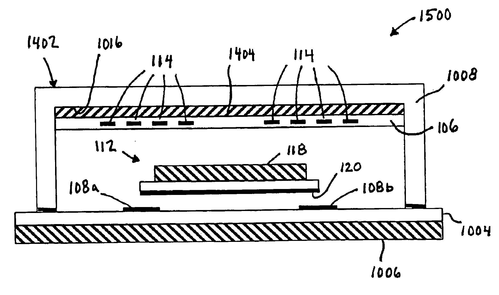
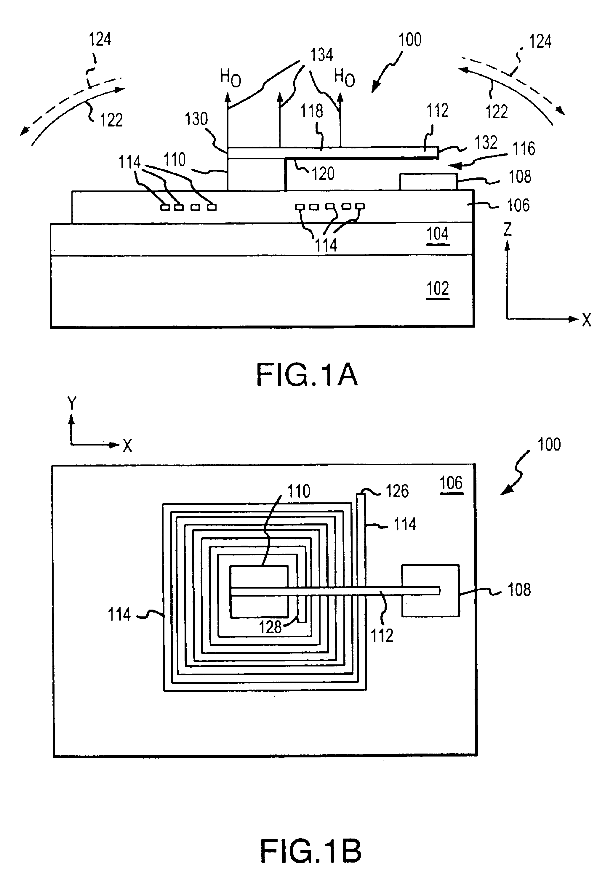
Packages for a micromachined magnetic latching switch, and methods for assembling the packages are described. In one aspect, a substrate is defined by opposing first and second surfaces. A micromagnetic switch integrated circuit (IC) chip is mounted to the first surface. A contact pad on the chip is coupled to a trace on the first surface. A permanent magnet is positioned closely adjacent to the chip. A cap is attached to the first surface. An inner surface of the cap forms an enclosure to enclose the chip on the first surface. The chip can be alternatively mounted to the inner surface of the cap. The chip can be oriented in a standard or flip-chip fashion. In another aspect, a moveable micro-machined cantilever is supported by a surface of a substrate. A cap is attached to the surface. An inner surface of the cap forms an enclosure that encloses the cantilever on the surface of the substrate. A permanent magnet is positioned closely adjacent to the cantilever. An electromagnet is attached to the inner surface or an outer surface of the cap.

Description

CROSS-REFERENCE TO RELATED APPLICATIONS[0001]This application claims the benefit of U.S. Provisional Application No. 60 / 291,651, filed May 18, 2001, which is herein incorporated by reference in its entirety.[0002]U.S. Non-provisional Application No. 10 / 126,291, titled “Latching Micro Magnetic Relay Packages and Methods of Packaging,” filed on Apr. 18, 2002, which claims the benefit of U.S. Provisional Application No. 60 / 322,841, filed Sep. 17, 2001, is herein incorporated by reference in its entirety.[0003]U.S. Non-provisional Application No. 10 / 147,918, titled “Apparatus Utilizing Latching Micromagnetic Switches,” filed on May 20, 2002, which claims the benefit of U.S. Provisional Application No. 60 / 291,651, filed May 18, 2001, is herein incorporated by reference in its entirety.BACKGROUND OF THE INVENTION[0004]1. Field of the Invention[0005]The present invention relates to electronic and optical switches. More specifically, the present invention relates to packaging of micromagnet...

Claims


Application Information

Patent Timeline
IPC IPC(8): H01H50/00H01H51/22
CPCH01H50/005H01H2050/007
Inventor SHEN, JUNGODAVARTI, PRASAD S.STAFFORD, JOHNTAM, GORDON
Owner SCHNEIDER ELECTRIC IND SAS
Learn More