
Electro-optical device having a concave recess formed above a substrate in correspondence with a plurality of wirings and an electro-optical apparatus having same

Inactive Publication Date: 2005-05-24
SEIKO EPSON CORP
View PDF35 Cites 44 Cited by
  • Summary
  • Abstract
  • Description
  • Claims
  • Application Information

AI Technical Summary

Benefits of technology

[0010]At all events, therefore, there are posed problems of more complicated manufacturing steps, a lower yield and a high cost.
[0041]A first insulating film may be deposited over the entire screen display area to form a multilayered portion on a first substrate. Then, a resist pattern corresponding to a concave recess may be formed by photolithography on the deposited first insulating film. Etching may be carried out via the resist pattern to remove the first insulating film corresponding to the concave recess. Then, a second insulating film may be deposited on the first insulating film and the area from which the first insulating film has been removed. As a result, the thickness of the first interlayer insulating film in the concave recess portion may be controlled relatively easily through control of the thickness of the second insulating film. When dry etching is used in this etching step, an aperture having substantially a designed exposure size can be provided.

Problems solved by technology

At all events, therefore, there are posed problems of more complicated manufacturing steps, a lower yield and a high cost.
This may result in an increase in step in the pixel section.
When such a storage capacitor is incorporated in an area under the data lines or along the scanning lines, thickness in this portion may increase causing production of a large step.
This may result in a step of about 10,000 Å. Thus, flattening applied for offsetting the step in the image display area may be difficult and expensive.

Method used


Image

  • Electro-optical device having a concave recess formed above a substrate in correspondence with a plurality of wirings and an electro-optical apparatus having same
  • Electro-optical device having a concave recess formed above a substrate in correspondence with a plurality of wirings and an electro-optical apparatus having same
  • Electro-optical device having a concave recess formed above a substrate in correspondence with a plurality of wirings and an electro-optical apparatus having same

Examples


Embodiment Construction

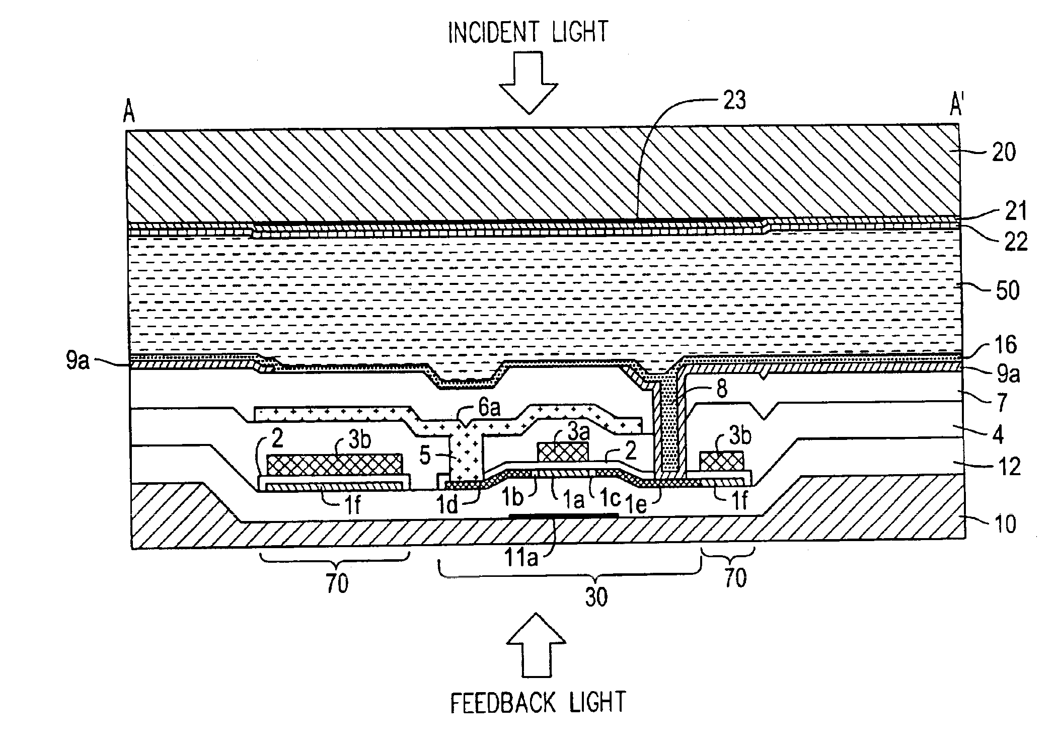
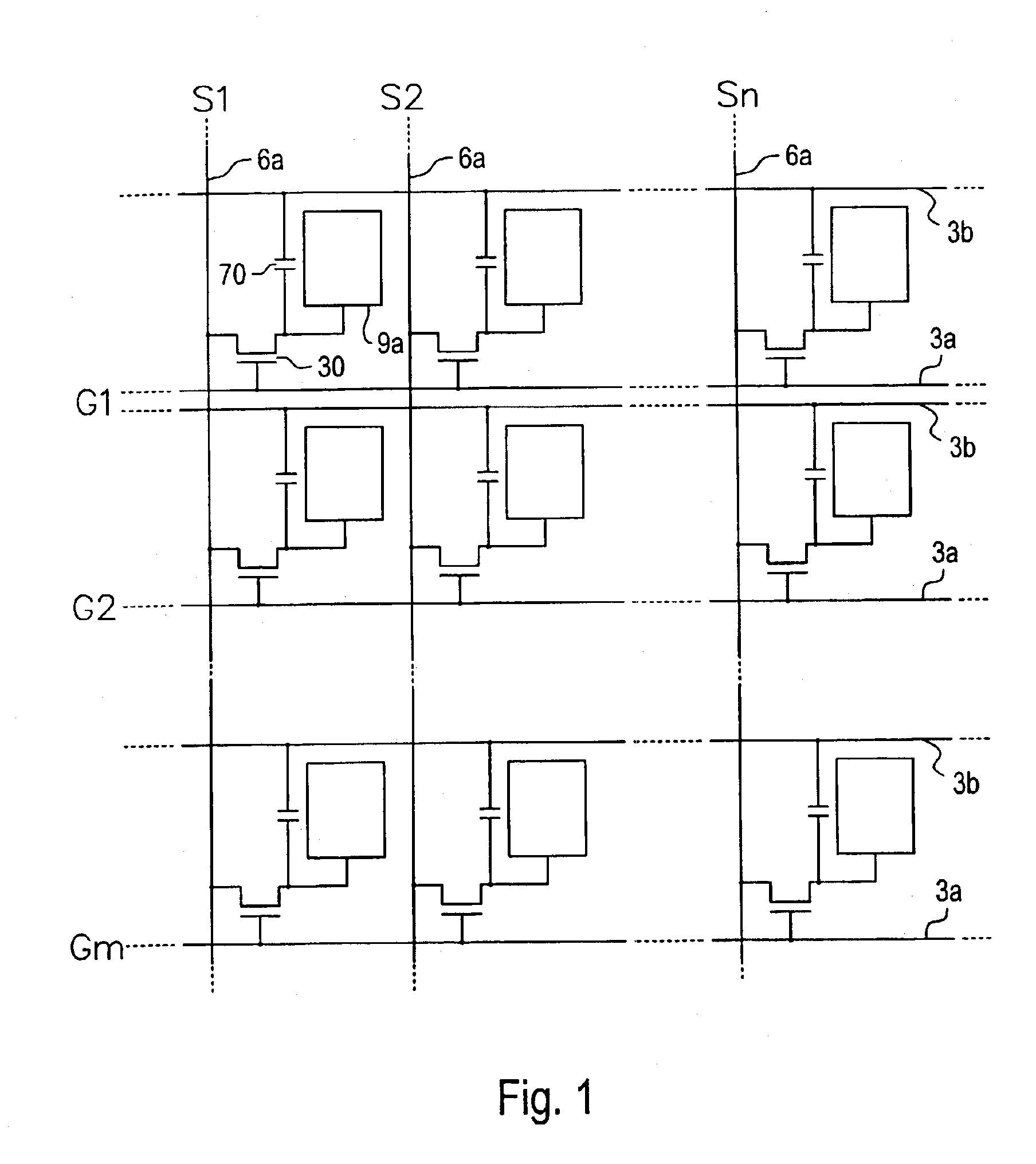
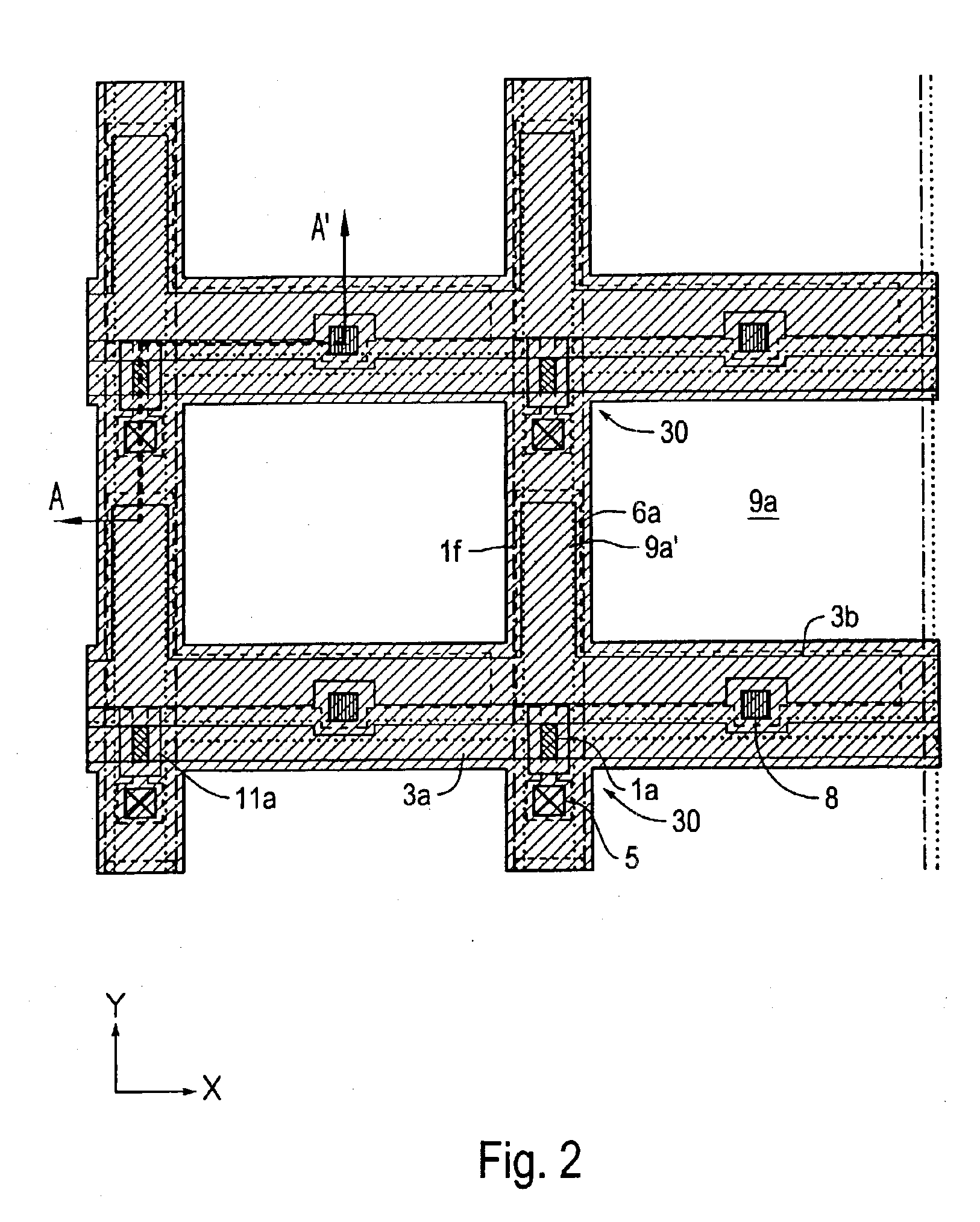
[0131]A configuration of the electro-optical apparatus of the present invention in the image display area and operations thereof will now be described with reference to FIGS. 1 to 4. FIG. 1 illustrates an equivalent circuit of various elements and wiring lines provided in a plurality of matrix-shaped pixels forming an image display area. FIG. 2 is a plan view illustrating a plurality of pixels adjacent to each other on a TFT array substrate having data lines, scanning lines, pixel electrodes and light shielding films formed thereon. FIG. 3 is a sectional view of FIG. 2 along the line A-A′. FIG. 4 is a sectional view corresponding to the A-A′ sectional view of FIG. 2. In FIGS. 3 and 4, layers and elements are shown in different reduced scales to make the components recognizable.

[0132]As shown in FIG. 1, the plurality of pixels are formed into a matrix shape so as to form the image display area of the electro-optical apparatus. This may include a pixel electrode 9a, a TFT 30 for contr...


PUM


Abstract

An electro-optical device includes a concave recess formed above a substrate, in correspondence with a plurality of wirings.

Description

[0001]This is a Continuation of application Ser. No. 10 / 153,804, filed May 24, 2002 now U.S. Pat. No. 6,611,301, which in turn is a continuation of application Ser. No. 09 / 216,872 filed Dec. 21, 1998 now U.S. Pat. No. 6,433,841. The entire disclosure of the prior application is hereby incorporated by reference herein in its entirety.BACKGROUND OF THE INVENTION[0002]1. Field of the Invention[0003]The present invention relates to an active matrix driven or passive matrix driven electro-optical apparatus such as a liquid crystal apparatus based on thin-film transistor driving or thin-film diode driving, a manufacturing method thereof, and an electronic device using the same.[0004]2. Description of Related Art[0005]A liquid crystal apparatus typically includes an electro-optical apparatus, a pair of alignment films that are rubbed in prescribed directions and provided on a pixel electrode and an opposing electrode between a pair of substrates, and an electro-optical material such as liq...

Claims


Application Information

Patent Timeline
IPC IPC(8): G02F1/13G02F1/1362G09G3/36G02F1/1333
CPCG02F1/13454G02F1/136227G09G3/3648G02F1/136209G02F1/1333G09G2320/0223
Inventor MURADE, MASAOYONEYAMA, RYOICHI
Owner SEIKO EPSON CORP
Learn More