System for correcting aberrations and distortions in EUV lithography

a technology of aberration and distortion, applied in the field of extreme ultraviolet (euv) lithography, can solve the problems of degrading the optical performance of euv lithography tools, affecting the quality of images at the wafer, and affecting the quality of images,

Inactive Publication Date: 2005-05-24
NIKON CORP
View PDF22 Cites 41 Cited by
  • Summary
  • Abstract
  • Description
  • Claims
  • Application Information

AI Technical Summary

Problems solved by technology

A number of factors can degrade optical performance of EUV lithography tools.
Manufacturing errors in the projection optics mirrors, as well as thermally induced deformations in their illuminated regions during operation, can produce optical aberrations which will degrade image quality at the wafer.
Image placement errors (distortion) can also occur.
Since the reticle illumination is non-telecentric, changes in reticle height (caused for example by non-flatn

Method used


Image

  • System for correcting aberrations and distortions in EUV lithography
  • System for correcting aberrations and distortions in EUV lithography
  • System for correcting aberrations and distortions in EUV lithography

Examples


Embodiment Construction

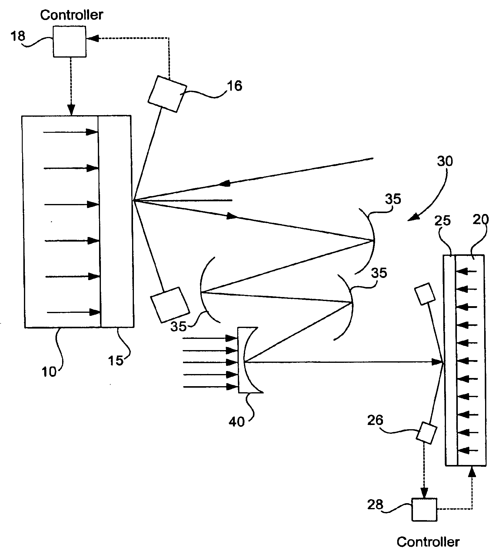
[0024]FIG. 4 shows schematically an EUV lithographic projection apparatus incorporating an aberration and distortion correcting system of this invention. EUV radiation from a source (not shown) is made incident on a reticle 15 set on a deformable reticle chuck 10, and reflected radiation from the reticle 15 is focused on a wafer 25 set on a deformable wafer chuck 20 by means of an optical system 30 including a plurality of intermediate reflectors 35 and a deformable mirror 40 serving as the last-stage reflector located proximally to the exit pupil (not shown) of the optical system 30. Numerals 16 and 26 respectively indicate a reticle height sensor and a wafer height sensor. Controller 18 processes the information from reticle height sensor 16 and adjusts the deformable reticle chuck 10. Controller 28 plays a similar role for the wafer height sensor 26 and deformable wafer chuck 20.

[0025]The theory of aberrations in a diffraction-limited system is described e.g. in Born and Wolf, Pr...


PUM

PropertyMeasurementUnit
Heightaaaaaaaaaa
Deformation enthalpyaaaaaaaaaa
Electrostatic attractive forceaaaaaaaaaa

Abstract

A system for correcting aberration and distortion in EUV lithography places a reticle on a deformable reticle chuck, and a reticle height sensor is used to measure the surface height of the reticle placed on the deformable reticle chuck. An optical system projects EUV radiation onto the reticle and collects and projects reflected EUV radiation from the reticle through its exit pupil onto a wafer placed on a wafer chuck. A deformable mirror disposed proximal to the exit pupil may also be controlled for this purpose. The deformable reticle chuck and the deformable mirror are controlled such that aberration and distortion of an image of the reticle formed on the wafer by the optical system are corrected based on the height measured by the reticle height sensor. The deformable reticle chuck includes a supporting structure, a deformable membrane disposed above and being comprised of a dielectric layer and a conductive layer, a voltage source connected to the conductive coating on the reticle and the conductive layer to generate an electrostatic attractive force between them, a plurality of actuator rods each connected to a corresponding one of actuators, and a coolant gas inside a chamber formed between the membrane and the top surface of the supporting structure. A deformable wafer chuck and wafer height sensor may be included to provide further correction of the image.

Description

[0001]This applications claims benefit to U.S. Provisional application Ser. No. 60 / 391,059 filed Jun. 21, 2002, and claims benefit to U.S. Provisional application Ser. No. 60 / 390,880 filed Jun. 21, 2002.BACKGROUND OF THE INVENTION[0002]This invention is in the technical field of extreme ultraviolet (EUV) lithography.[0003]A number of factors can degrade optical performance of EUV lithography tools. Manufacturing errors in the projection optics mirrors, as well as thermally induced deformations in their illuminated regions during operation, can produce optical aberrations which will degrade image quality at the wafer. Image placement errors (distortion) can also occur. Since the reticle illumination is non-telecentric, changes in reticle height (caused for example by non-flatness of the reticle) can also produce distortion at the wafer.[0004]It is therefore an object of this invention to provide a system for correcting aberration and distortion in EUV lithography, or a lithographic p...

Claims


Application Information

Patent Timeline
IPC IPC(8): G03F7/20G03F7/207H01L21/027
CPCG03F7/70233G03F7/70258G03F7/70266G03F7/703G03F7/70708G03F7/70783G03F7/70875G03F7/70891G03F7/707Y10T428/24802
Inventor SOGARD, MICHAEL
Owner NIKON CORP
Why Eureka
Try Eureka