Method and structure for a high voltage junction field effect transistor

a junction field effect transistor and high-voltage technology, applied in the direction of transistors, semiconductor devices, electrical equipment, etc., can solve the problems of igbts and mosfets bjts are susceptible to thermal runaway, and igbts and mosfets have the disadvantage of being susceptible to gate damage, etc., to available charge carriers, enhance the breakdown resistance of the device, and minimize the electric potential gradien

Inactive Publication Date: 2005-05-31
POWER INTEGRATIONS INC
View PDF28 Cites 12 Cited by
  • Summary
  • Abstract
  • Description
  • Claims
  • Application Information

AI Technical Summary

Benefits of technology

[0007]A method for fabricating a junction field transistor for high-voltage applications is disclosed. A lightly doped first epitaxial layer is formed on a highly doped substrate. A second epitaxial layer is deposited with a heavier dopant concentration than the first epitaxial layer and a control structure having a plurality of implanted gate regions and a source. A guard ring is formed to isolate the source and the control structure. The combination of the lightly doped first epitaxial layer and the guard ring enable the JFET to be reliably operated with a breakdown voltage in excess of 100 volts.
[0008]In an embodiment of the present invention, a lightly doped epitaxial N− layer is deposited on an N+ silicon substrate. A second nominally doped N epitaxial layer is then deposited on top of the lightly doped epitaxial N− layer. P+ gate regions are implanted in the second epitaxial layer and source contacts are provided by forming N+ regions on a portion of the N epitaxial layer. The control structure resides within the second layer. The lightly doped first layer provides a drift region that increases the breakdown voltage between the drain and source and the drain and gate control structure. The top contacts and the bottom of the substrate are used as the source and drain contacts for the JFET.
[0009]In another embodiment of the present invention, A JFET is fabricated as described above, and a guard ring is provided to enhance the breakdown resistance of the device. The guard ring is formed by surrounding the control structure with P+ doped region that extends across the entire thickness of the N layer and into the N− layer. The width of the guard ring and the interface between the guard ring and the N− layer are designed to minimize the electric potential gradient and available charge carriers along paths other than the desired current path.

Problems solved by technology

However, the supply voltage between the drain and source (Vds) is usually relatively low.
IGBTs and MOSFETs have the disadvantage of being susceptible to gate damage due to static discharge, and BJTs are susceptible to thermal runaway.

Method used


Image

  • Method and structure for a high voltage junction field effect transistor
  • Method and structure for a high voltage junction field effect transistor
  • Method and structure for a high voltage junction field effect transistor

Examples


Embodiment Construction

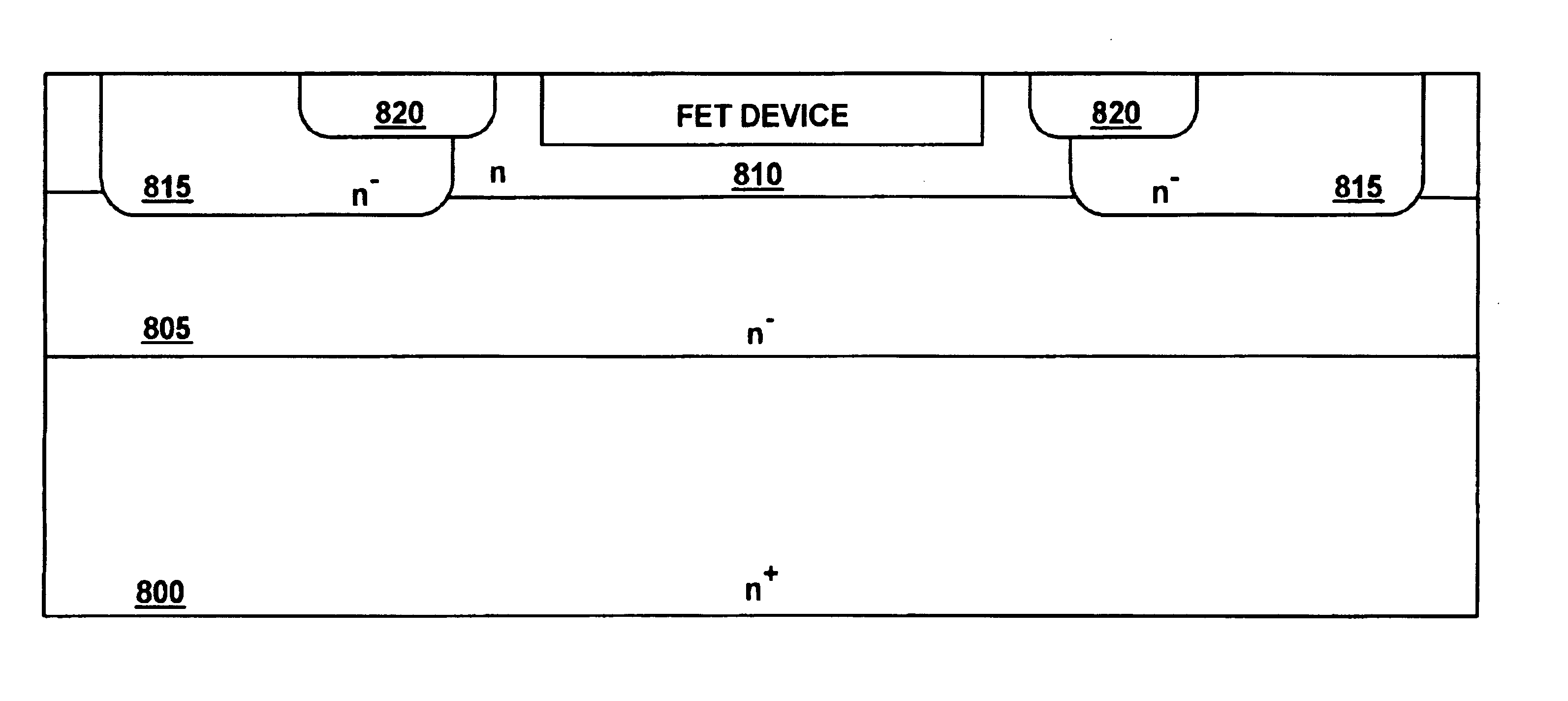
[0026]In the following detailed description of the present invention, a high voltage junction field effect transistor (JFET) structure and a method for fabricating the structure; numerous specific details are set forth in order to provide a thorough understanding of the present invention. However, it will be obvious to one skilled in the art that the present invention may be practiced without these specific details. In other instances well known methods involving deposition, photolithography, etch, etc., and well known structures such as ohmic contacts, barrier metallization, etc., have not been described in detail so as not to unnecessarily obscure aspects of the present invention.

[0027]U.S. Pat. No. 6,251,716 entitled “JFET Structure and Manufacture Method for Low On-Resistance and Low Voltage Application,” issued Jun. 26, 2001, and assigned to the assignee of the present invention, is hereby incorporated herein by reference.

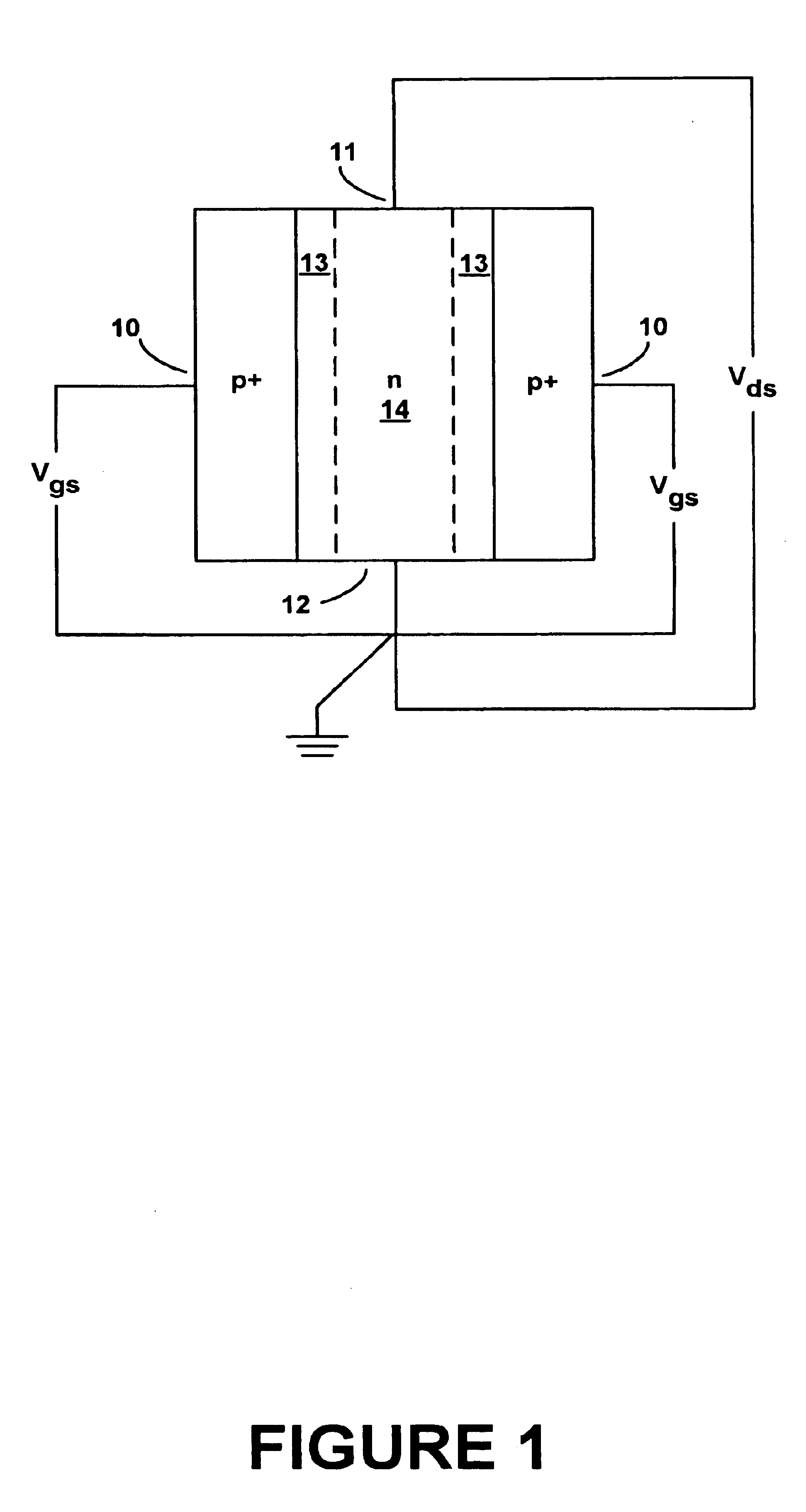
[0028]FIG. 1 shows a general schematic for an n-channel ...


PUM


Abstract

A method for fabricating a junction field transistor for high-voltage applications. A lightly doped first epitaxial layer is formed on a highly doped substrate. A second epitaxial layer is deposited with a heavier dopant concentration than the first epitaxial layer. The second layer contains a control structure having a plurality of implanted gate regions and a source. A guard ring is formed to isolate the source and the control structure. The combination of the lightly doped first epitaxial layer and the guard ring enable the JFET to be operated with a breakdown voltage in excess of 100 volts. Multiple guard rings may be used to provide a breakdown voltage in excess of 150 volts.

Description

FIELD OF THE INVENTION[0001]Embodiments of the present invention relate to the field of junction field effect transistors (JFETs). In particular, embodiments of the present invention relate to a high voltage JFET.BACKGROUND ART[0002]Junction field effect transistors (JFETs) are majority carrier devices that conduct current through a channel that is controlled by the application of a voltage to a p-n junction. JFETs may be constructed as p-channel or n-channel and may be operated as enhancement mode devices or depletion mode devices.[0003]The most common JFET type is the depletion mode type. The depletion mode device is a normally “on” device that is turned off by reverse biasing the p-n junction so that pinch-off occurs in the conduction channel. P-channel depletion mode devices are turned off by the application of a positive voltage between the gate and source (positive Vgs), whereas n-channel depletion mode devices are turned off by the application of a negative voltage between th...

Claims


Application Information

Patent Timeline
Patent Type & Authority Patents(United States)
IPC IPC(8): H01L21/337H01L21/02H01L29/06H01L21/338H01L29/66H01L29/02H01L29/812H01L29/808
CPCH01L29/0619H01L29/0692H01L29/8122H01L29/66909H01L29/8083H01L29/66848
Inventor YU, HO-YUANJOHNSON, ERIC
Owner POWER INTEGRATIONS INC
Why Eureka
Try Eureka