
Clock generator with programmable non-overlapping-clock-edge capability

a clock generator and clock edge technology, applied in the field of program, can solve the problems of avoiding the need for costly and time-consuming trial and error design and redesign of on-chip clock generators, and achieve the effect of optimizing the chip performance, widening the tolerance, and widening the toleran

Inactive Publication Date: 2005-05-31
SAMSUNG ELECTRONICS CO LTD
View PDF36 Cites 18 Cited by
  • Summary
  • Abstract
  • Description
  • Claims
  • Application Information

AI Technical Summary

Benefits of technology

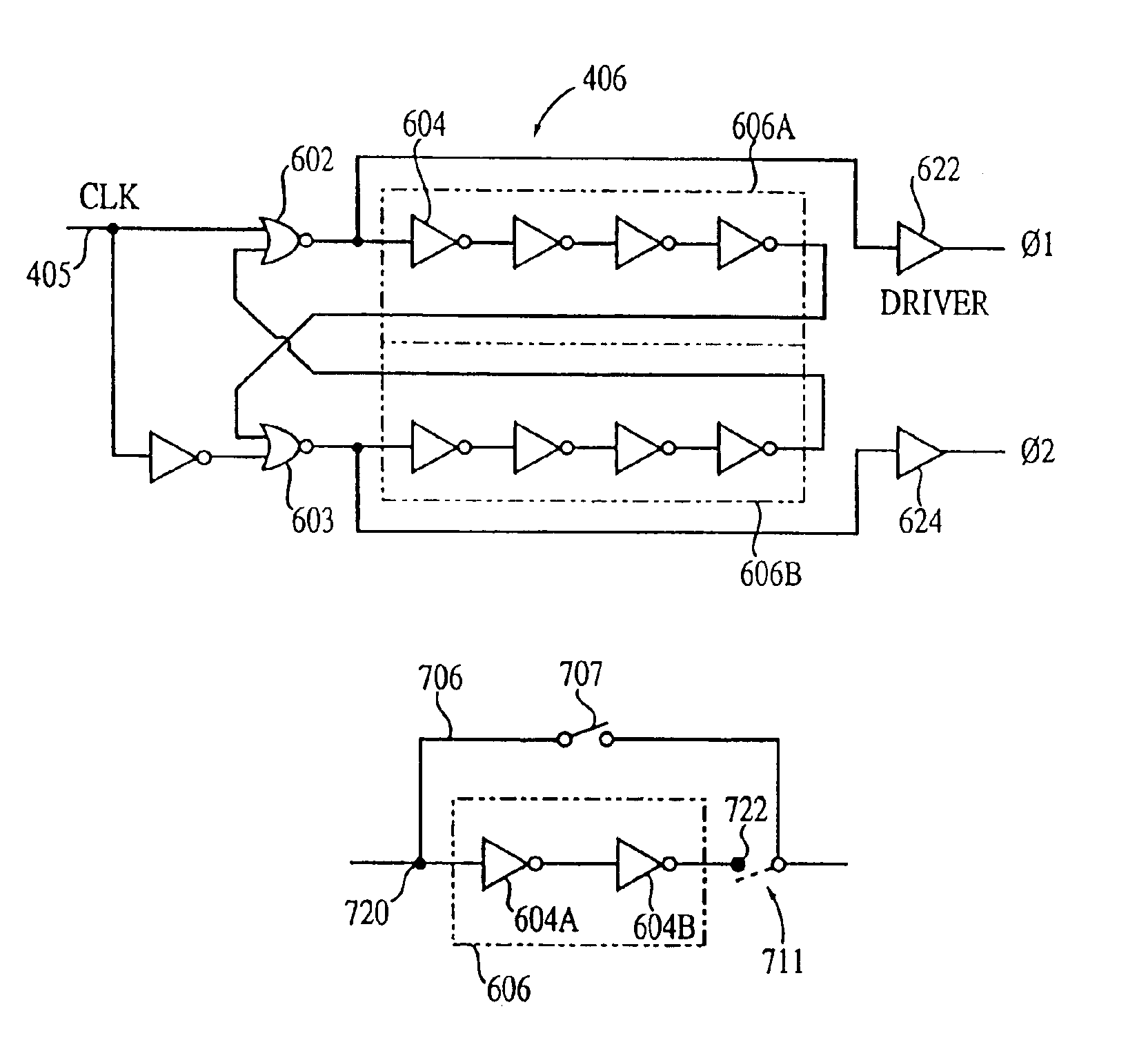
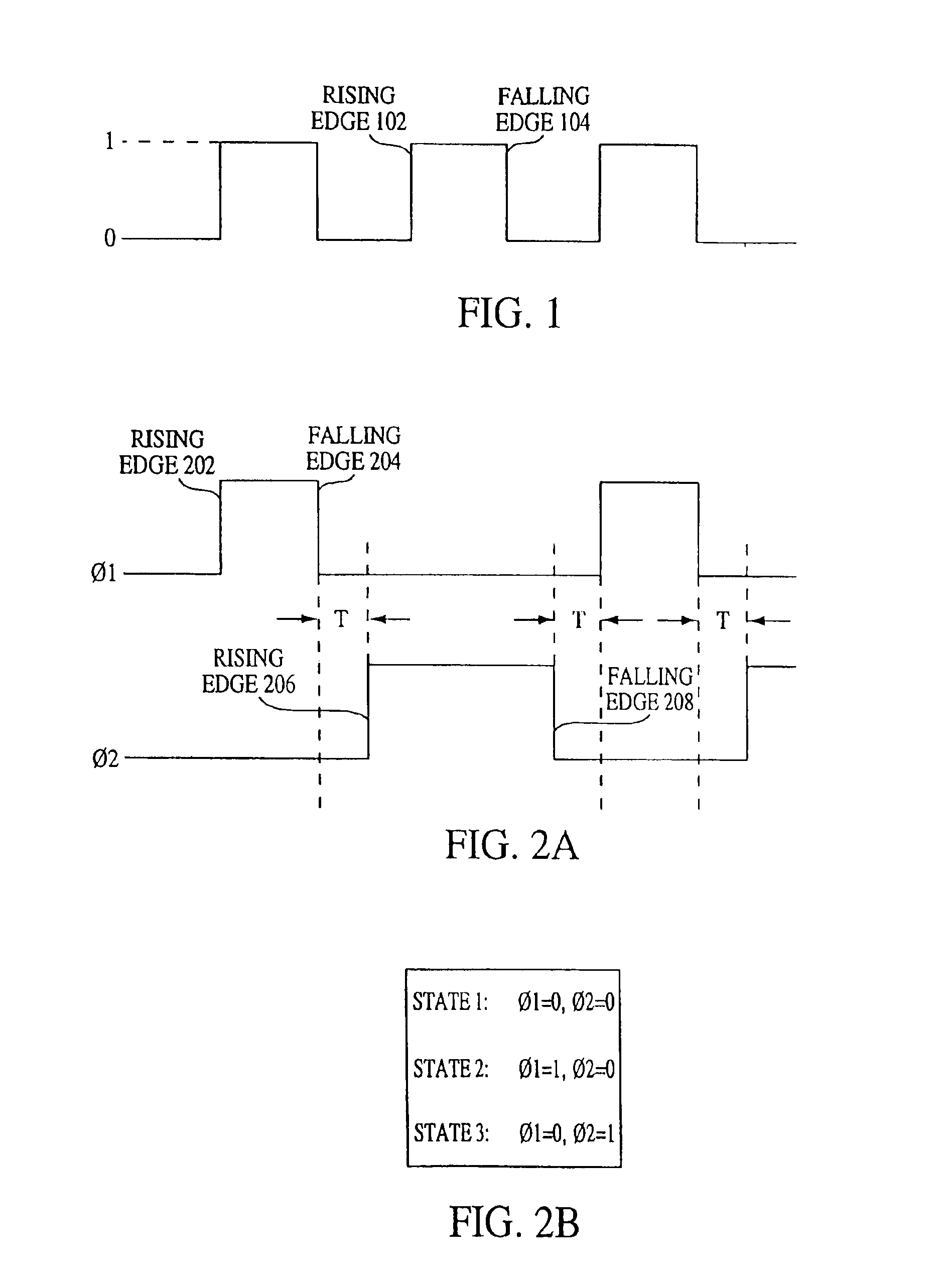
[0014]The programmable on-chip clock generator provides two phases of a system clock with non-overlapping edges. The programmability of the clock generator provides flexibility during chip fabrication, and when a chip is functioning in a operational environment.
[0015]During the manufacturing phases of chip production, characteristics of the on-chip clock generator are altered to ensure the edges of the two generated clocks do not overlap. This allows the manufacturer to optimize the performance of the chip while the chip is undergoing initial production testing. This feature obviates the need to perform costly and time consuming trial-and-error design and redesign of on-chip clock generators.
[0016]Additionally, the present invention provides a technique for optimizing the performance of the on-chip clock generator after the chips have left the manufacturing environment. One feature of the present invention is the ability to adjust clock generation dynamically to account for climatic changes in an operational, or other post-production, environment. This allows chips to be manufactured with wider tolerances and allows operation of the chip to be optimized when the chip is in the operational environment.

Problems solved by technology

This feature obviates the need to perform costly and time consuming trial-and-error design and redesign of on-chip clock generators.

Method used


Image

  • Clock generator with programmable non-overlapping-clock-edge capability
  • Clock generator with programmable non-overlapping-clock-edge capability
  • Clock generator with programmable non-overlapping-clock-edge capability

Examples


Embodiment Construction

I. General Overview

[0032]A. Brief Overview

[0033]The present invention is directed to a system and method for providing non-overlapped clock generation on a chip. The present invention includes four main embodiments. The first embodiment is directed to the overall operation of an on chip clock generator. The second embodiment is directed to a hardware programmable clock generation system and method. The third embodiment is directed to a software programmable clock generation system and method. The fourth embodiment is directed to a combination of the first three embodiments.

[0034]These embodiments of the present invention are discussed in the following sections.

[0035]B. Environment

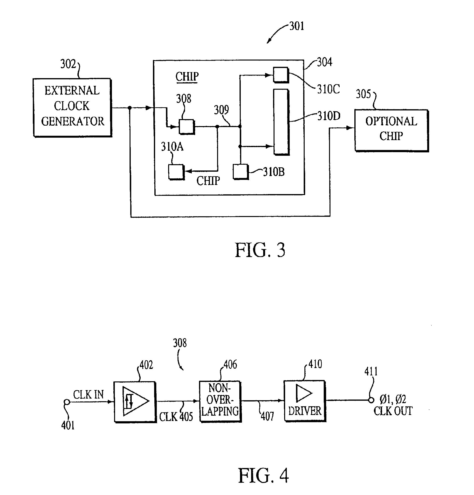
[0036]FIG. 3 illustrates a high level block diagram of an environment 301 in which the present invention operates. Environment 301 may be a wafer containing hundreds of chips at a fabrication / testing stage or a computer in a user environment. As illustrated, environment 301 includes an external clock genera...


PUM


Abstract

A system and method for generating and optimizing clock signals with non-overlapping edges on a chip using a unique programmable on-chip clock generator. Overlapping of the edges of the clocking signals is avoided by adjusting an amount of delay introduced in the on-chip clock generator circuit. The amount of delay is adjusted by programming the on-chip clock generator using either hardware and / or software programming. In hardware programming, the amount of delay adjusted by physically altering the composition of delay elements in the on-chip clock generator. In software programming, the delay is adjusted using software commands to control the operation of delay elements in the on-chip clock generator, or to select the paths that delay the signals.

Description

CROSS-REFERENCE TO RELATED APPLICATIONS[0001]This is a continuation of application Ser. No. 10 / 277,757, filed Oct. 23, 2002, now U.S. Pat. No. 6,653,881 which is a continuation of application Ser. No. 09 / 970,773, filed Oct. 5, 2001, now U.S. Pat. No. 6,489,826, which is a continuation of application Ser. No. 09 / 726,035 filed Dec. 1, 2000, now U.S. Pat. No. 6,323,711, which is a continuation of application Ser. No. 09 / 376,186, filed Aug. 17, 1999, now U.S. Pat. No. 6,163,194, which is a continuation of application Ser. No. 08 / 795,363, filed Feb. 4, 1997, now U.S. Pat. No. 5,966,037, which is a continuation of application Ser. No. 08 / 478,534, filed Jun. 7, 1995, now abandoned, which is a division of application Ser. No. 08 / 255,910, filed Jun. 8, 1994, U.S. Pat. No. 5,444,405, which is a continuation of application Ser. No. 07 / 967,614, filed Oct. 28, 1992, now abandoned, which is a continuation-in-part of application Ser. No. 07 / 844,066, filed Mar. 2, 1992, now abandoned.BACKGROUND OF ...

Claims


Application Information

Patent Timeline
Patent Type & Authority Patents(United States)
IPC IPC(8): H03K5/15H03K5/151
CPCH03K5/1515H03K2005/00058
Inventor TRUONG, HO DAILIN, CHONG MING
Owner SAMSUNG ELECTRONICS CO LTD
Learn More