
Image sensor and pixel reading method used this image sensor

a technology of image sensor and pixel reading, which is applied in the direction of color television details, television system, color signal processing circuit, etc., can solve the problem of processing the optical black region b>40/b>, which must be changed, and achieve the effect of increasing the accuracy of the black level and simplifying the structure of the camera system

Inactive Publication Date: 2005-05-31
NEC ELECTRONICS CORP
View PDF14 Cites 68 Cited by
  • Summary
  • Abstract
  • Description
  • Claims
  • Application Information

AI Technical Summary

Benefits of technology

[0019]It is therefore an object of the present invention to provide an image sensor and a pixel reading method used this image sensor, in which the accuracy of a black level can be increased by that an optical black region being the black level reference of signals is read every horizontal line at a local or random access mode, and also the structure of a camera system used this image sensor can be simplified.
[0026]According to the present invention, at the pixel reading method used the image sensor, when the local or random access mode is activated, pixels in the optical black region being the black level for signals to be read are read every horizontal line. That is, the pixels in the selected horizontal line in the pixel reading region are read, and after this, one or more pixels in the same selected horizontal line in the optical black region are read. Therefore, an effect that the accuracy of the black level is increased can be obtained.
[0027]According to the present invention, the process for the optical black region can be the same between the frame access mode in which the OB cells are automatically read every horizontal line because all the pixels are read and the local access mode or the random access mode in which a certain number of OB cells are surely read until the horizontal line ends. Therefore, an effect that the structure of the camera system can be simplified is obtained.

Problems solved by technology

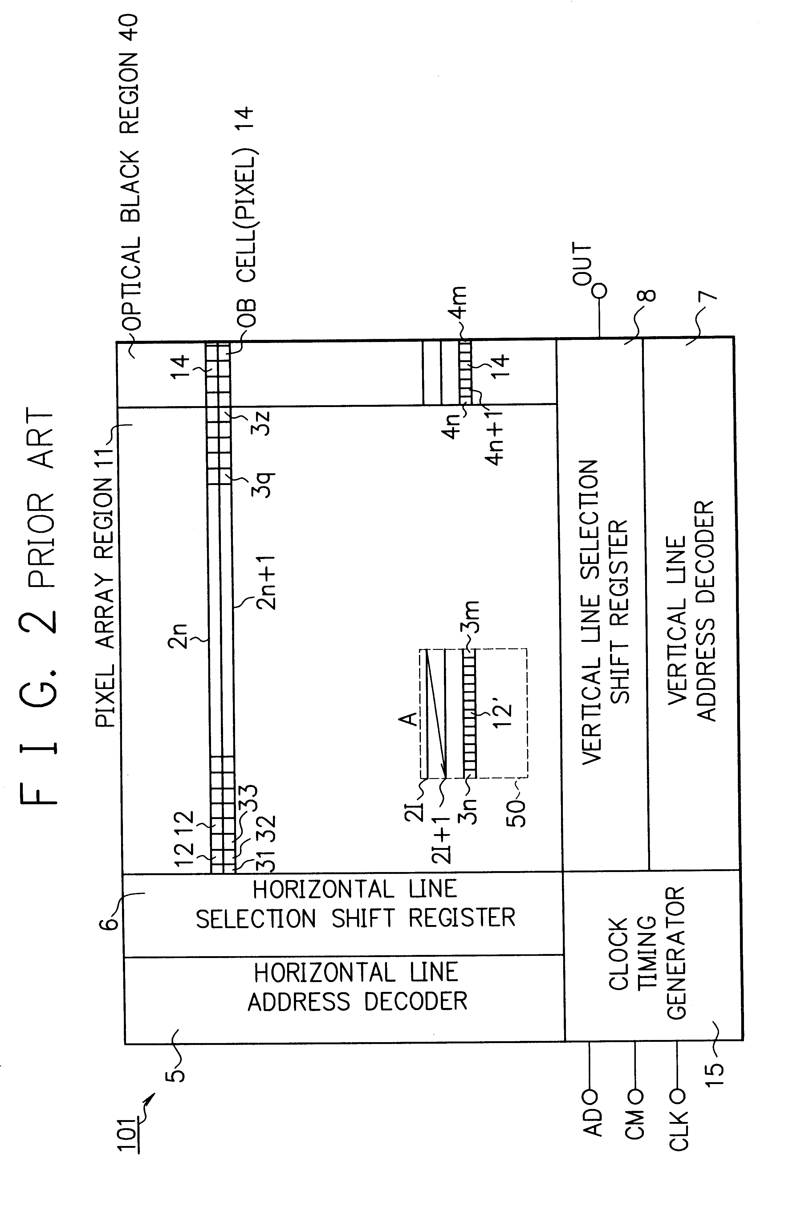
At the frame access process, the optical black region 40 is read every horizontal line, however, at the local (or random) access mode, the optical black region 40 is not read every horizontal line, therefore there is a disadvantage that a process handling the optical black region 40 must be changed at the local (or random) access mode.

Method used


Image

  • Image sensor and pixel reading method used this image sensor
  • Image sensor and pixel reading method used this image sensor
  • Image sensor and pixel reading method used this image sensor

Examples


first embodiment

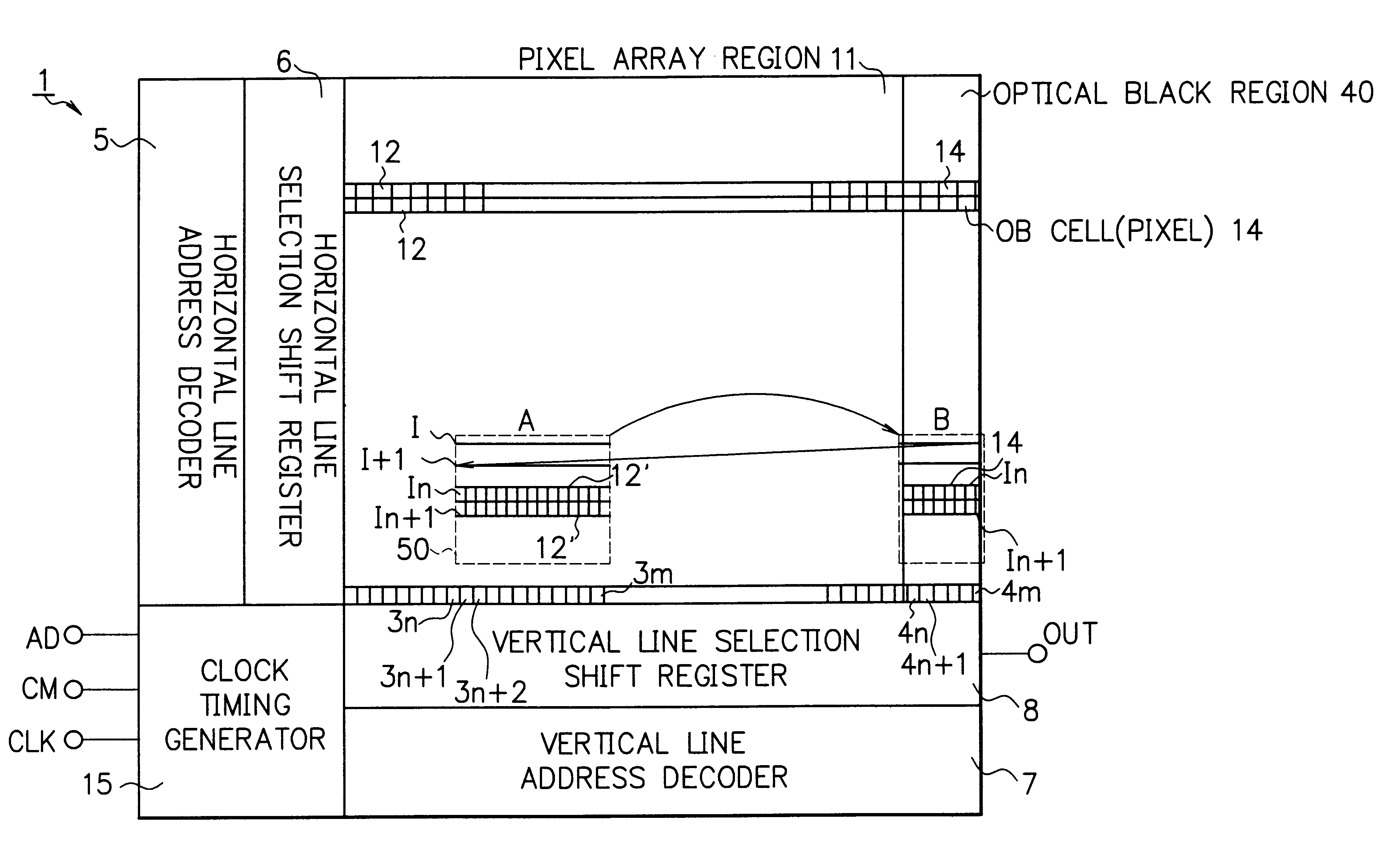
[0036]Referring to FIGS. 4, and 5, the present invention is explained.

[0037]The MOS type image sensor 1 provides a pixel array region 11 and an optical black region 40 disposed in the one end part of the pixel array region 11. When the mode selector 41 selects a local access mode or a random access mode, the MOS type image sensor 1 decides a pixel reading region 50 in which one or more pixels 12 to be read are disposed in the pixel array region 11. And the MOS type image sensor 1 reads information in one or more pixels 12′ disposed in a horizontal line address I selected in the pixel reading region 50 every selected one horizontal line address I. After this, the MOS type image sensor 1 reads information in one or more pixels 14 in the selected horizontal line address I in the optical black region 40. In this, the pixels 12′ are the pixels 12 in the pixel reading region 50.

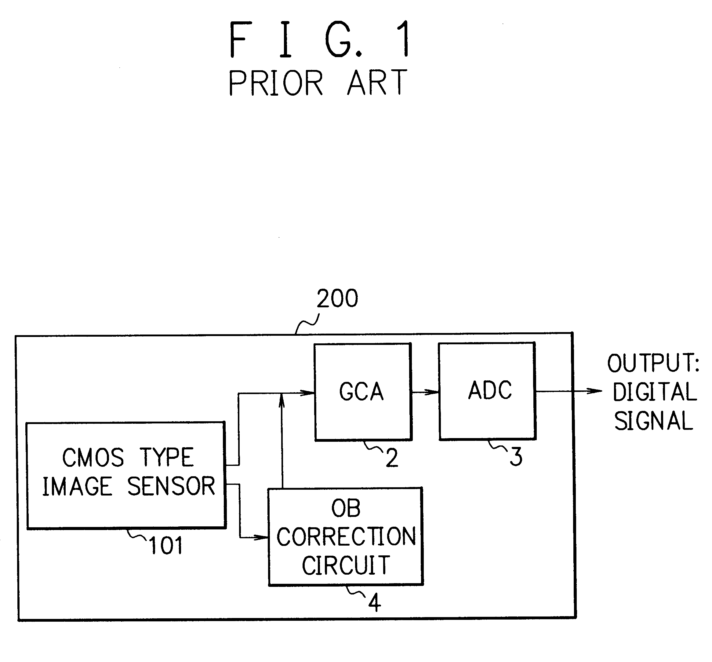
[0038]The structure of the camera system 100 used the MOS type image sensor 1 is explained in more detail. First...

second embodiment

[0059]Therefore, at the second embodiment, the vertical line finished flag F is also outputted to the OB correction circuit 4 in the camera system 100. And by using this vertical line finished flag F as a trigger, the reading start information of the optical black region 40 is inputted to the OB correction circuit 4. With this, regardless of the difference of the number of pixels 12′ of one horizontal line, the camera system 100 can know the reading start timing of the optical black region 40. Therefore, the camera system 100 can be simplified.

[0060]At the second embodiment, the vertical line finished flag F is used as the trigger for the reading start signal of the OB correction circuit 4. However, a reading start selection signal of an arbitrary optical black region 40 can be used as an OB reading trigger inputting to the OB correction circuit 4.

[0061]Further, at the first and second embodiments of the present invention, the optical black region 40 is disposed at the right end in ...


PUM


Abstract

An image sensor and a pixel reading method used this image sensor, in which the accuracy of a black level can be increased by that an optical black region being the black level reference of signals is read every horizontal line at a local or random access mode, are provided. And also the structure of a camera system used this image sensor can be simplified is provided. The image sensor is a MOS type image sensor composed of a pixel array region and an optical black region disposed at the one end in the pixel array region. And the MOS type image sensor provides a mode selector that selects the local access or random access mode or a frame access mode. When the local access or random access mode is activated, the image sensor decides a pixel reading region in the pixel array region. The image sensor reads information of one or more pixels having a designated horizontal line address in the pixel reading region every horizontal line address. After this, the MOS type image sensor reads information of one or more pixels having the same designated horizontal line address in the optical black region.

Description

BACKGROUND OF THE INVENTION[0001]The present invention relates to an image sensor and a pixel reading method used this image sensor, in particular, in which a metal oxide semiconductor (MOS) type image sensor, which is capable of adopting a local access mode or a random access mode in addition to a frame access mode, is used.DESCRIPTION OF THE RELATED ART[0002]A MOS type image sensor is different from a charge coupled device (CCD) image sensor that needs a specified manufacturing process, and can be manufactured by a standard MOS manufacturing process. And the MOS type image sensor has a low power consumption characteristic by its low voltage and single power source operation. And further the MOS type image sensor has an advantage that its peripheral logic circuit and macro circuit can be formed in one chip. Therefore, the MOS type image sensor has been largely studied.[0003]FIG. 1 is a block diagram showing a structure of a camera system used a conventional complementary metal oxid...

Claims


Application Information

Patent Timeline
Patent Type & Authority Patents(United States)
IPC IPC(8): H04N5/217H04N1/407H04N25/00
CPCH04N5/374H04N5/361H04N25/76H04N25/633H04N25/78H04N25/63
Inventor MURAMATSU, YOSHINORINIKOU, HIDEMITSU
Owner NEC ELECTRONICS CORP
Learn More