Circuits and methods for screening for defective memory cells in semiconductor memory devices

a technology of memory cells and circuits, applied in electronic circuit testing, digital storage, instruments, etc., can solve the problems of increasing the testing time and abnormal leakage current flowing through the memory cells, and achieve the effect of efficient screening for defective or weak memory cells

Inactive Publication Date: 2005-05-31
SAMSUNG ELECTRONICS CO LTD
View PDF15 Cites 50 Cited by
  • Summary
  • Abstract
  • Description
  • Claims
  • Application Information

AI Technical Summary

Benefits of technology

[0008]The present invention is directed to circuits and methods for efficientl

Problems solved by technology

This demand applies to static random access memory devices (SRAMs), for example, where physical damage and topological miss-alignments in cell areas can generate defective memory cells.
Defective or weak memory cells can result in abnormal leakage current flowing

Method used


Image

  • Circuits and methods for screening for defective memory cells in semiconductor memory devices
  • Circuits and methods for screening for defective memory cells in semiconductor memory devices
  • Circuits and methods for screening for defective memory cells in semiconductor memory devices

Examples


Embodiment Construction

[0022]In the following description, exemplary embodiments of the invention are discussed in detail to provide a thorough understanding of the present invention. It is to be understood, however, that the description of preferred embodiments is for purposes of illustration and that nothing herein should be construed as placing any limitation of the invention. Indeed, it will be apparent to those of ordinary skill in the art that present invention may be practiced without these specific details

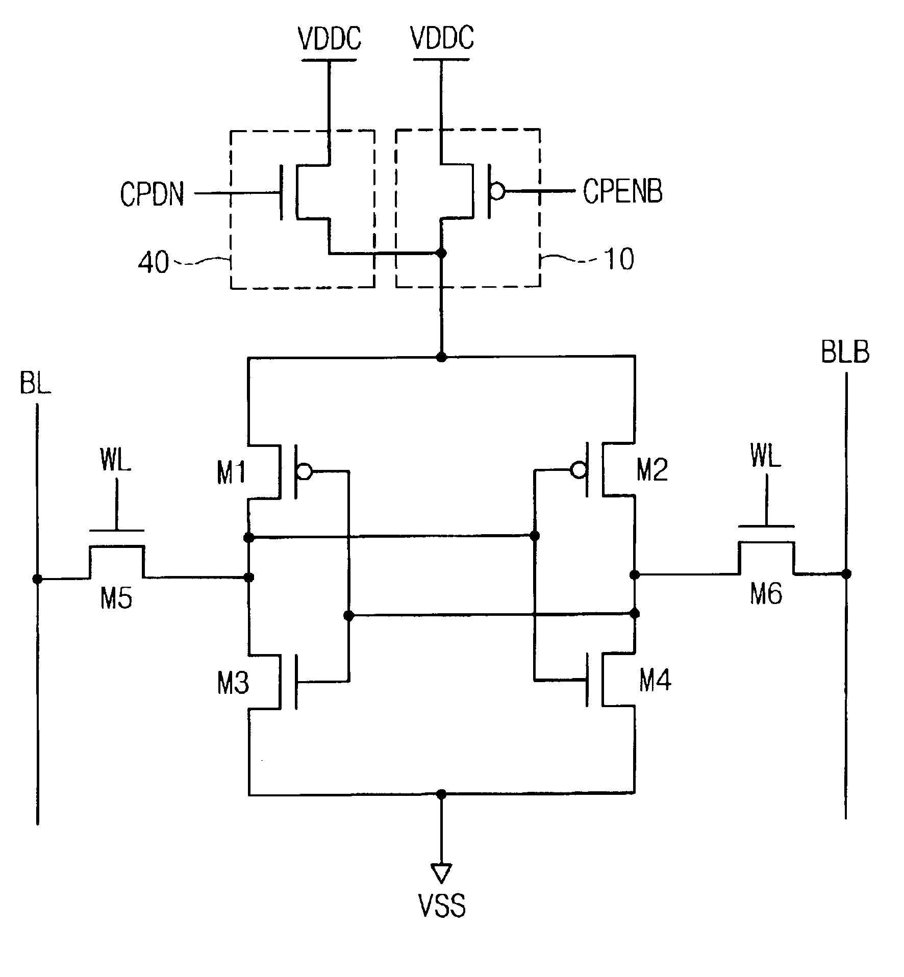
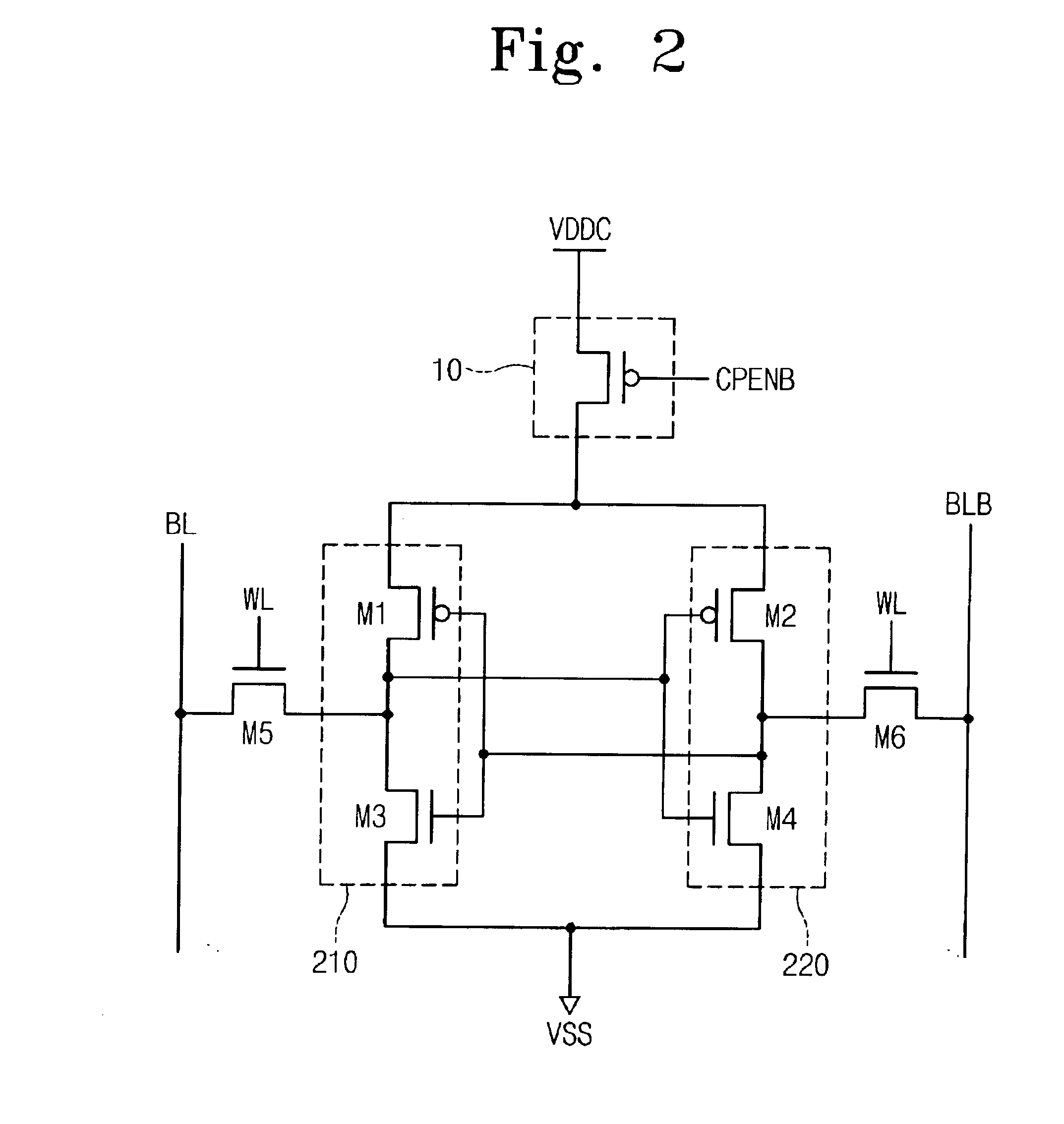
[0023]FIG. 2 illustrates a circuit construction that is used for screening a SRAM cell according to an embodiment of the present invention. Referring to FIG. 2, a SRAM cell comprises a CMOS-type cell, including PMOS transistors M1 and M2, and NMOS transistors M3˜M6. The transistors M1˜M4 are cross-coupled with their gates, drains, and sources to form latch circuits 210, 220, as is well known in the art. Each NMOS transistor M5 and M6 is connected to a respective bitline BL and BLB, and has a gate...


PUM


Abstract

Circuits and methods that enable screening for defective or weak memory cells in a semiconductor memory device. In one aspect, a semiconductor memory device comprises first and second drivers for a SRAM cell. The first driver is connected between a power supply voltage and the cell, which supplies the power supply voltage into the cell in response to a cell power control signal. The second driver is connected between the power supply signal and the cell, which supplies a voltage lower than the power supply voltage into the cell in response to the cell power down signal. A method for screening for defective or weak cells does not require a time for stabilizing a circuit condition after voltage variation to supply the voltage lower than the power supply voltage from a conventional tester because the cell power down signal activates a driver that causes a supply voltage that is lower than the power supply voltage to be loaded directly to the cell, which results in a reduction of the test time for screening defective cells.

Description

CROSS-REFERENCE TO RELATED APPLICATION[0001]This application claims priority to Korean Patent Application No. 2002-29200, filed on May 27, 2002, which is incorporated herein by reference.FIELD OF THE INVENTION[0002]The present invention generally relates to semiconductor memory devices and, more specifically, to circuits and methods that enable screening for defective or weak memory cells in a semiconductor memory device.BACKGROUND OF THE INVENTION[0003]Due to the demand for increased data storage capacity and density of memory cells of semiconductor memory devices, such devices are being designed with smaller design rules. This demand applies to static random access memory devices (SRAMs), for example, where physical damage and topological miss-alignments in cell areas can generate defective memory cells. Defective or weak memory cells can result in abnormal leakage current flowing through the memory cells during standby states. Efficient and accurate methods for detecting or scree...

Claims


Application Information

Patent Timeline
IPC IPC(8): G11C29/04G11C29/50G01R31/28G11C11/413G11C29/00G11C29/06
CPCG11C29/12005G11C29/50G11C11/41G11C2029/5006G11C2029/5002G11C29/00
Inventor SON, YOUNG-JAECHO, UK-RAELEE, KWANG-JIN
Owner SAMSUNG ELECTRONICS CO LTD
Why Eureka
Try Eureka