
Transportable container including an internal environment monitor

a technology of environment monitor and transportable container, which is applied in the direction of semiconductor/solid-state device testing/measurement, packaged goods type, instruments, etc., can solve the problems of contamination of semiconductor wafers, substantially interfering with 1 m geometry semiconductor devices, and particle damage in semiconductor processing

Inactive Publication Date: 2005-06-07
ENTEGRIS INC
View PDF14 Cites 66 Cited by
  • Summary
  • Abstract
  • Description
  • Claims
  • Application Information

AI Technical Summary

Benefits of technology

[0066]It is a further advantage of the present invention that data from transportable pods can be used to gather information about individual process tools in the fabrication facility, and can also identify the source of a particular contaminant within the fabrication facility. If it is evident over time that pods frequently exhibit abnormal readings after processing at a particular tool, an embodiment of the present invention identifies this situation and the tool may be taken off-line for inspection and maintenance. While prior art systems allow for testing and monitoring of wafer lots, this is performed either by manually or automatedly taking the pods to a metrology tool, where the pods are opened and the workpieces tested for contaminants. Not only do embodiments of the present invention perform such testing on a continuous basis, they do so in a non-invasive manner without having to open the pods and without slowing the processing throughput of the wafer lot.

Problems solved by technology

Particles can be very damaging in semiconductor processing because of the small geometries employed in fabricating semiconductor devices.
Unwanted contamination particles which have geometries measuring greater than 0.1 μm substantially interfere with 1 μm geometry semiconductor devices.
There are several sources that cause contamination of semiconductor wafers as they travel through a fabrication process.
For example, during a manufacturing process, certain gases, fluids, pressures, coherent and incoherent light, vibrations, electrostatic charge, and contaminants may affect the final yield of semiconductors.
Each of these operations and pod features can be potential sources of contaminants to semiconductor wafers within a pod.
While such operations are capable of identifying problems after they occur, known testing systems are not intended to pinpoint the time or location at which the problems occur.
Thus, such testing operations are often performed too late to prevent contamination to a wafer lot.
Moreover, where a contaminated pod is allowed to continue through the fabrication process, it often contaminates other processing tools and wafer lots.
Further still, conventional testing operations are not intended to identify the areas within the fabrication facility which are introducing contaminants to the wafers.

Method used


Image

  • Transportable container including an internal environment monitor
  • Transportable container including an internal environment monitor
  • Transportable container including an internal environment monitor

Examples


Embodiment Construction

[0028]Embodiments of the present invention are described hereinafter with respect to SMIF pods for carrying semiconductor wafers within a semiconductor wafer fabrication process. However, it is understood that embodiments of the present invention may be used with transportable containers other than SMIF pods. For example, embodiments of the present invention may be used with unsealed semiconductor lot boxes, pods for transporting workpieces other than semiconductor wafers, such as, for example, reticles and flat panel displays, etc. It is further understood that embodiments of the present invention comply with and allow compliance with all applicable SEMI standards. However, it is contemplated that alternative embodiments of the present invention not comply with the SEMI standards.

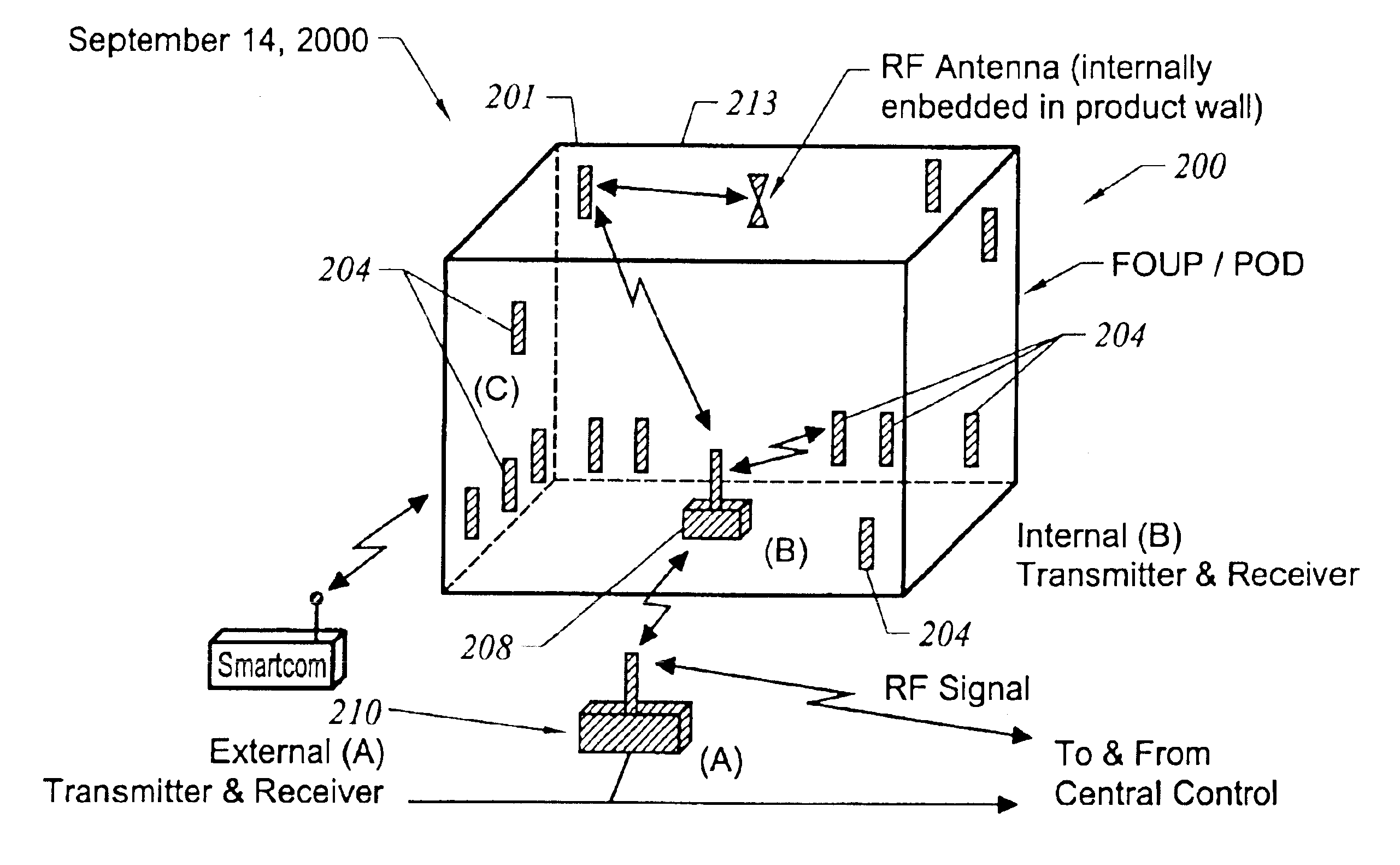
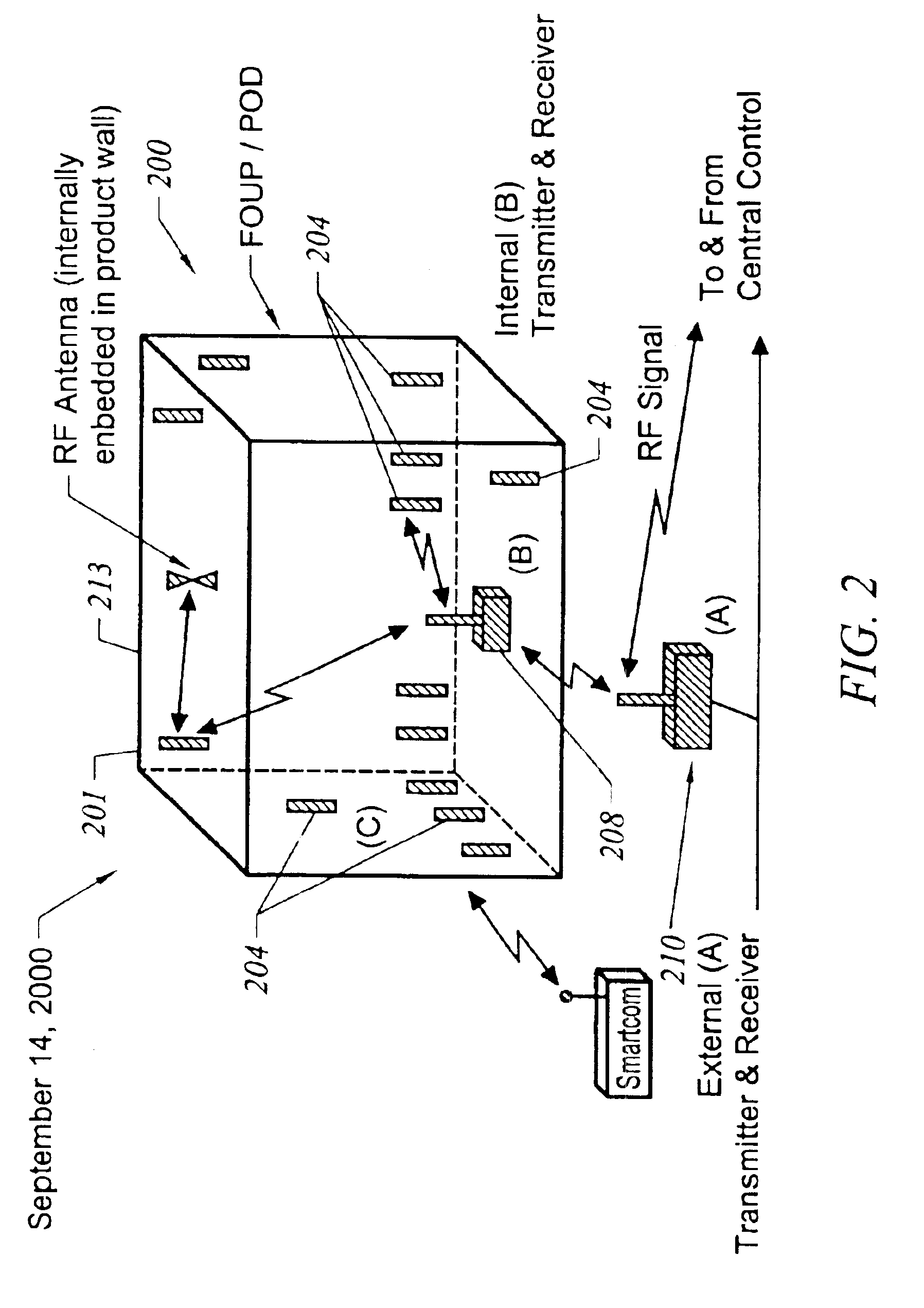
[0029]FIG. 2 illustrates a block diagram of an embodiment of a transportable pod monitoring system 200 including a transportable pod 201, and an internal sensor network 202. Various embodiments of transpor...


PUM

PropertyMeasurementUnit
Frequencyaaaaaaaaaa
Frequencyaaaaaaaaaa
Temperatureaaaaaaaaaa

Abstract

A system is disclosed allowing non-invasive, continuous local and remote sensing of the internal environmental characteristics of transportable containers. The system utilizes a variety of sensors inside the container to sense internal environmental conditions.

Description

CLAIM OF PRIORITY[0001]This application claims priority to U.S. Provisional patent application No. 60 / 261,035, filed Jan. 10, 2001, entitled SMART POD INCLUDING ONBOARD MONITORING SYSTEM, incorporated herein by reference.BACKGROUND[0002]1. Field of the Invention[0003]The present invention relates to the manufacture of semiconductor wafers, and in particular to a system allowing non-invasive, continuous local and remote sensing of the internal environmental characteristics of transportable containers.[0004]2. Description of Related Art[0005]A Standard Mechanical Interface (“SMIF”) system proposed by the Hewlett-Packard Company is disclosed in U.S. Pat. Nos. 4,532,970 and 4,534,389. The purpose of a SMIF system is to reduce particle fluxes onto semiconductor wafers (“wafers”) during storage and transport of the wafers through the semiconductor fabrication process. This purpose is accomplished, in part, by mechanically ensuring that during storage and transport, the gaseous media (such...

Claims


Application Information

Patent Timeline
IPC IPC(8): B65B3/04B65B1/04B65G65/00B65D25/02B65G1/00B67C3/02H01L21/68H01L21/67H01LH01L21/00H01L21/673
CPCG03F7/7075H01L21/67393H01L21/67253Y10S414/14H01L22/00
Inventor SPEASL, JERRY A.DANTE, EDWARD
Owner ENTEGRIS INC
Learn More