Semiconductor memory device capable of controlling potential level of power supply line and/or ground line

a memory device and semiconductor technology, applied in the direction of information storage, static storage, digital storage, etc., can solve the problems of not reducing the power consumption of the semiconductor memory device during the operation cannot be reduced, and the power consumption of the semiconductor memory device cannot be reduced. to achieve the effect of reducing power consumption

Inactive Publication Date: 2005-06-07
RENESAS ELECTRONICS CORP
View PDF10 Cites 77 Cited by
  • Summary
  • Abstract
  • Description
  • Claims
  • Application Information

AI Technical Summary

Benefits of technology

[0011]An object of the present invention is to provide a semiconductor memory device capable of reducing power consumption caused by a charging / discharging current of a bit line or the like as well as caused by a gate leakage current of a memory cell in a non-selected column.
[0019]Therefore, according to the present invention, power consumption by a charging / discharging current of a bit line or the like as well as by a gate leakage current of a memory cell in a non-selected column can be reduced.

Problems solved by technology

Therefore, lowering of power consumption during the operation is not expected.
Generally, power consumed during operation of the semiconductor memory device is the sum of power consumption by charging / discharging current of a bit line or the like and power consumption by the leakage current.
On the other hand, these semiconductor memory devices cannot reduce power consumption by the charging / discharging current of the bit line or the like, which is one factor of the power consumption during operation.

Method used


Image

  • Semiconductor memory device capable of controlling potential level of power supply line and/or ground line
  • Semiconductor memory device capable of controlling potential level of power supply line and/or ground line
  • Semiconductor memory device capable of controlling potential level of power supply line and/or ground line

Examples


embodiment 1

[0062

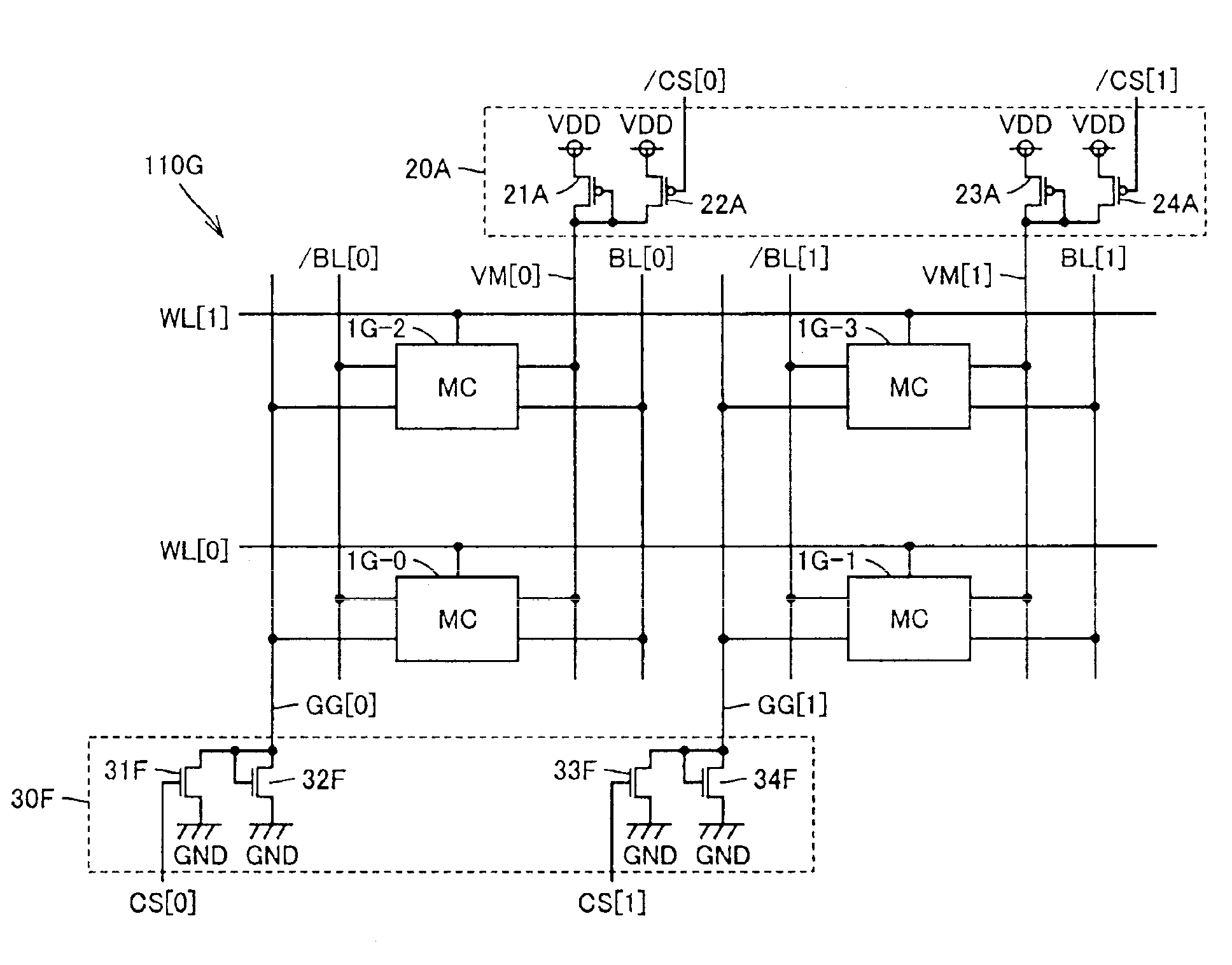
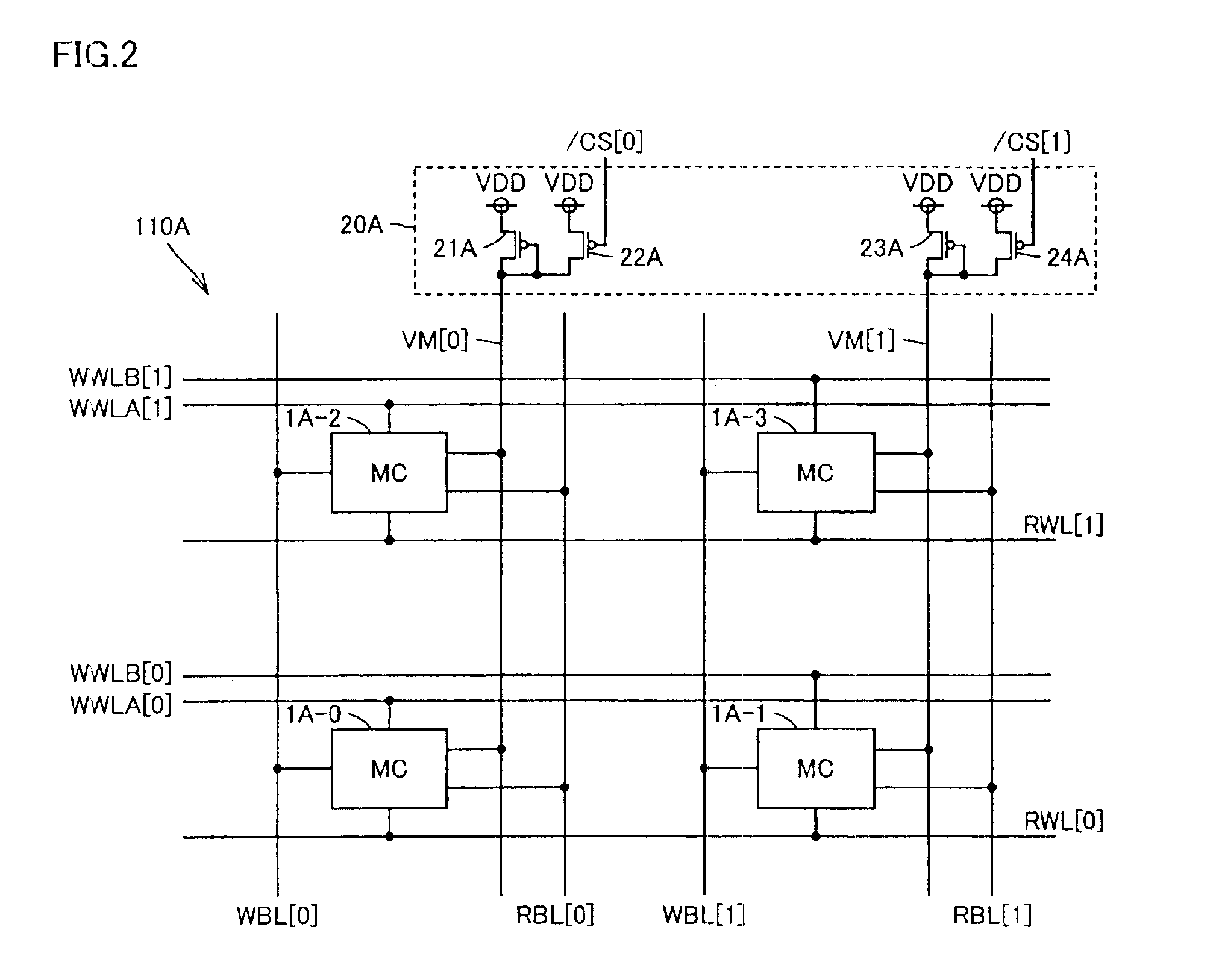
[0063]FIG. 2 is a circuit diagram showing a circuit configuration of a memory cell array 110A and its periphery in Embodiment 1 of the present invention. Memory cell array 110A of Embodiment 1 shown in FIG. 2 has a memory cell array configuration of two rows and two columns, for example.

[0064]Referring to FIG. 2, memory cell array 110A in Embodiment 1 includes memory cells 1A-0, 1A-1, 1A-2, 1A-3 arranged in matrix of rows and columns, write word lines WWLA[0], WWLA[1], WWLB[0], WWLB[1] and read word lines RWL[0], RWL[1] arranged in a direction of row, and write bit lines WBL[0], WBL[1] and read bit lines RBL[0], RBL[1] arranged in a direction of column.

[0065]Write word lines WWLA[0], WWLB[0] are connected to memory cells 1A-0, 1A-1 respectively, whereas write word lines WWLA[1], WWLB[1] are connected to memory cells 1A-2, 1A-3 respectively. In this manner, in memory cell array 110A of Embodiment 1, a separate write word line is allocated to each memory cell, even if memory cell...

embodiment 2

[0129

[0130]FIG. 9 is a circuit diagram showing a circuit configuration of a memory cell array 110B and its periphery in Embodiment 2 of the present invention.

[0131]Referring to FIG. 9, memory cell array 10B in Embodiment 2 includes memory cells 1B-0, 1B-1, 1B-2, 1B-3 arranged in matrix of rows and columns, write word lines WWLA[0], WWLA[1], WWLB[0], WWLB[1] and read word lines RWL[0], RWL[1] arranged in a direction of row, and write bit lines WBL[0], WBL[1] and read bit lines RBL[0], RBL[1] arranged in a direction of column.

[0132]As a connection relation of the write word line, the read word line, the write bit line, and the read bit line to each memory cell is similar to that in memory cell array 110A in Embodiment 1, description thereof will not be repeated.

[0133]Memory cell array 110B in Embodiment 2 is connected to a power supply line level control circuit 20B via power supply lines VM1[0], VM2[0], VM1[1], VM2[1]. Each of power supply lines VM1[0], VM2[0] is connected in common ...

embodiment 3

[0147

[0148]FIG. 11 is a circuit diagram showing a circuit configuration of a memory cell array 110C in Embodiment 3 of the present invention.

[0149]Referring to FIG. 11, memory cell array 110C in Embodiment 3 includes memory cells 1C-0, 1C-1, 1C-2, 1C-3 arranged in matrix of rows and columns, write word lines WWLA[0], WWLA[1], WWLB[0], WWLB[1] and read word lines RWL[0], RWL[1] arranged in a direction of row, and write bit lines WBL[0], WBL[1] and read bit lines RBL[0], RBL[1] arranged in a direction of column.

[0150]As a connection relation of the write word line, the read word line, the write bit line, and the read bit line to each memory cell is similar to that in memory cell array 110A in Embodiment 1, description thereof will not be repeated.

[0151]In memory cell array 110C in Embodiment 3, level control signals / CS[0], / CS[1] are directly input to memory cells 1C-0, 1C-1, 1C-2, 1C-3. Level control signal / CS[0] is input in common to memory cells 1C-0, 1C-2, while level control si...


PUM


Abstract

Level control signals are both set to H level, and potentials of power supply lines are both set to be lower than a power supply potential. In this manner, a gate leakage current during waiting and writing operation of a memory cell array can significantly be reduced. The level control signals are set to L level and H level respectively, and solely the potential of one of the power supply lines is set to be lower than the power supply potential. In this manner, power consumption during a reading operation of the memory cell array can be reduced.

Description

BACKGROUND OF THE INVENTION[0001]1. Field of the Invention[0002]The present invention relates to a semiconductor memory device, and more particularly to a semiconductor memory device capable of holding storage data without a refresh operation.[0003]2. Description of the Background Art[0004]In a semiconductor memory device, in particular in an SRAM (Static Random Access Memory), power consumption can be lowered by controlling a source potential of a transistor constituting a memory cell so as to suppress a leakage current that flows between the source and the drain, for example.[0005]A conventional semiconductor memory device (a semiconductor device) disclosed in Japanese Patent Laying-Open No. 9-73784 reduces the leakage current by maintaining a reading speed by setting the source potential equal to a substrate potential during an operation, and by setting an absolute potential of the source to be higher than the substrate potential during waiting. Though the conventional semiconduc...

Claims


Application Information

Patent Timeline
Patent Type & Authority Patents(United States)
IPC IPC(8): G11C11/40G11C11/413G11C11/419G11C11/41G11C5/00G11C11/4193G11C5/14G11C11/34
CPCG11C5/14G11C11/417G11C11/413G11C5/147G11C7/1051G11C7/1078G11C11/419G11C7/18G11C8/14G11C2207/2227
Inventor NII, KOJI
Owner RENESAS ELECTRONICS CORP
Why Eureka
Try Eureka