[0018]The present invention provides an
image sensor device with low cost and high optical quality in a near
chip scale package based on standard
high density array format, quad flat no-lead (QFN)
assembly infrastructure. A tight tolerance in
assembly height and unique mechanical structure design provides close dimension matching with mold cavity height. The packaged sensor device uses an inner leadframe panel as a precise height standoff object to control the
focal length of the sensor. The lens is attached to its own leadframe panel with tape. The tape prevents resin bleeding, which keeps the lens clean and facilitates post-mold cleaning.
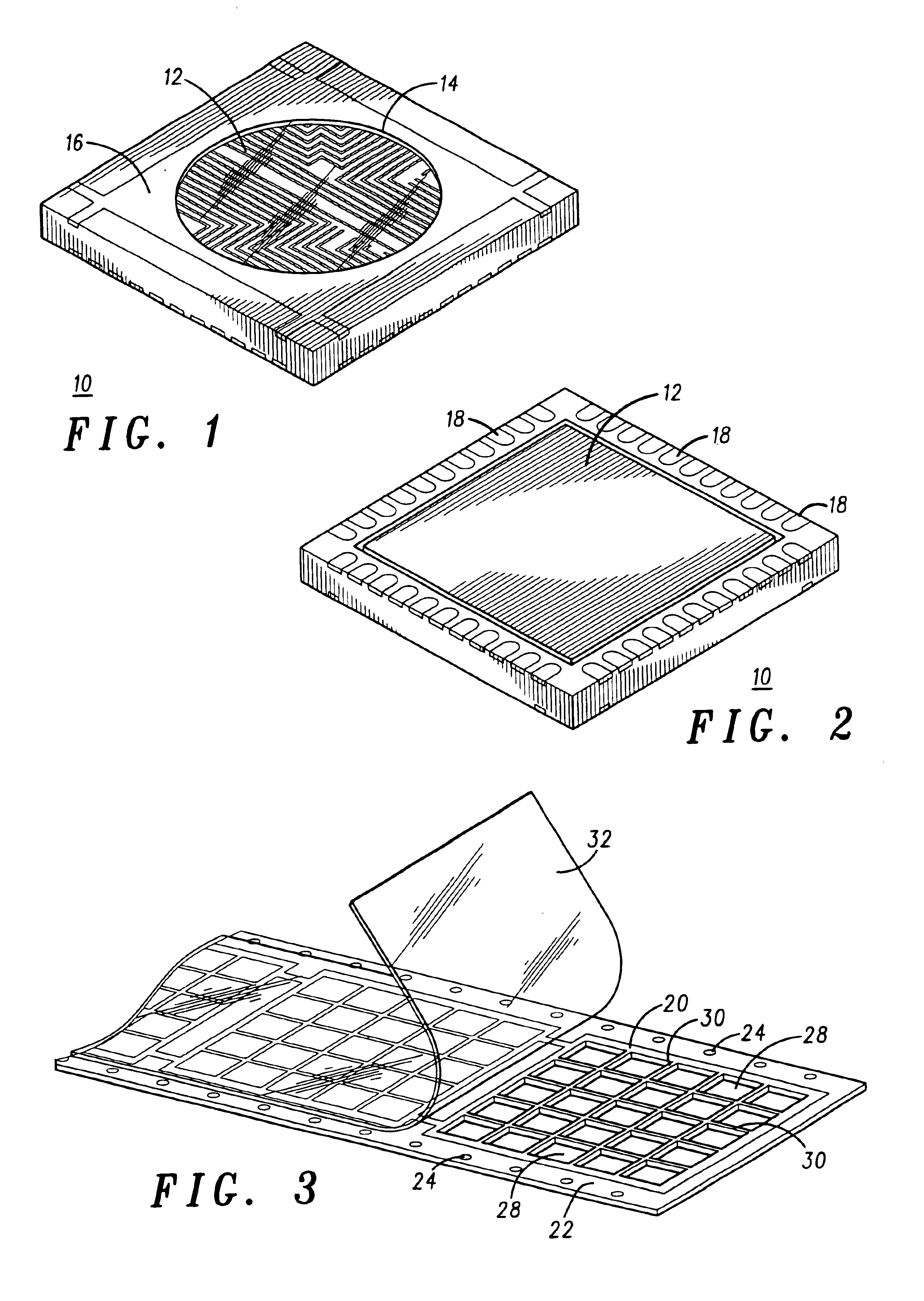
[0036]Referring to FIG. 1, an enlarged, top perspective view of a packaged optical sensor device 10 in accordance with the present invention is shown. The sensor device 10 preferably is a QFN (quad flat no-lead) type package. The QFN type package is preferred because of its
small form factor, low profile, and low
assembly cost. The sensor device 10 includes a sensor
integrated circuit (IC) 12 visible through a lens 14 that is fitted within a second leadframe 16. FIG. 2 is an enlarged, bottom perspective view of the optical sensor device 10, which shows a bottom side of the IC 12 and lead fingers 18 of a first leadframe 20 (see FIG. 3). The packaged device 10 is rectangular or square-shaped and the lens 14 is generally circular 14. However, the device 10 and lens are not limited to such shapes, as the shape of the package and the shape of the lens may vary.
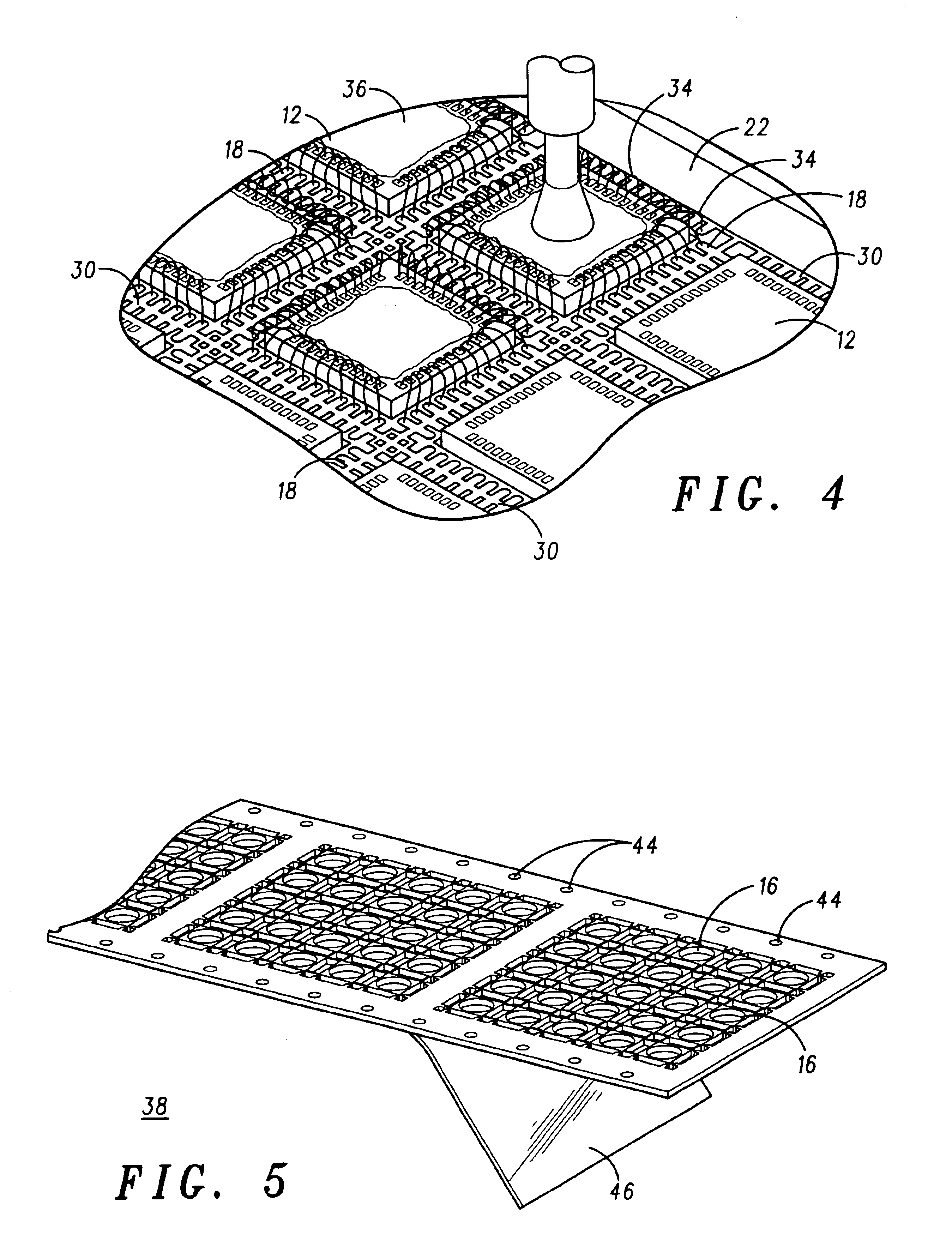
[0041]FIG. 6 is an enlarged perspective view of a step of placing the lenses 14 in the lens receiving areas 40 of the second leadframes 16 of the second leadframe panel 38. The lenses 14 may be clear plastic or glass. Preferably the lenses 14 are a non-reflective optical grade glass and have a thickness of about 15 to 16 mils. The lenses 14 may be coated with various materials to filter light, as desired. The lenses 14 are secured within the lens receiving areas 40 by an
adhesive on the surface of the second tape 46. Like the first leadframes 20, the ability to perform accurate and tight control in leadframe positional tolerance manufacturing allows the lenses 14 to be precisely located in the second leadframes 16.
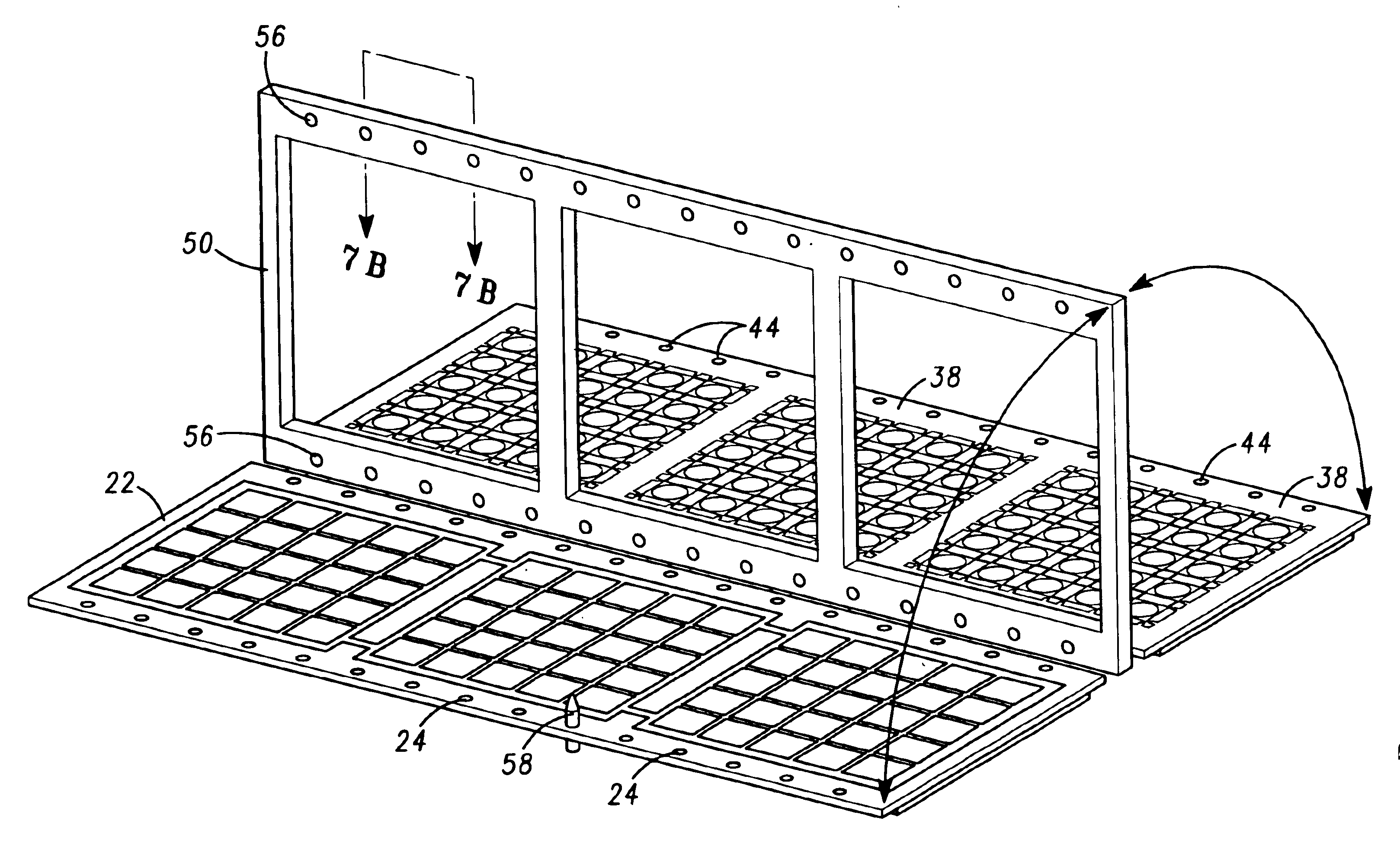
[0044]FIG. 8 is an enlarged perspective view showing a leadframe panel alignment step. In this step, the first, second and third leadframe panels 22, 38 and 50 are aligned by guide pins 58 inserted into the holes 24, 44 and 56 of the respective leadframe panels. The holes 24, 44 and 56 of the respective leadframe panels are located in identical locations around the respective panels to allow for precise alignment of the panels. Precisely aligning the panels, coupled with the very precise placement of both the ICs 12 and the lenses 14 provides precise alignment between the optical axes of the lenses 14 with the centers of the respective ICs 12, which is of critical importance in assembling
image sensor devices. As is known by those of skill in the art, misalignment of the
optical axis of the lens and sensor image circle center is the major cause of defects and thus yield loss in optical sensor manufacturing. By using leadframes for receiving both the ICs 12 and the lens 14, the present invention allows for very accurate placement and thus improved alignment accuracy. A
heat curing process may be performed to cure and harden the
adhesive globs 36, which the bonds the lenses 14 to the active areas of the ICs 12.
[0046]After injection of the mold compound 64 and curing, the first and second tapes 32 and 46 are removed from the first sides of the first and second leadframe panels 22 and 38. The first and second tapes 32 and 46 may be removed manually or with commercially available equipment. FIG. 10 shows the first tape 32 being removed from the first leadframe panel 22. The second tape 46 is removed in the same manner. The matrix of formed devices is then diced to form individual devices, as shown in FIG. 11. The dicing may be performed by sawing, as is known by those of skill in the art. FIG. 9 shows the locations with dashed lines 70 along which the leadframes may be
cut. In one embodiment, the image sensor device 10 has an overall height of about 40 mils. The lens 14 and clear
adhesive globs 36 allow light to pass therethrough and onto the active area of the sensor IC 12. Because the lenses 14 are covered by the second tale 46, resin bleeding onto the lenses is avoided. However, if any resin bleeding onto the lenses 14 should occur, a subsequent
water jet cleaning can be performed to remove such resin. The second tape 46 also avoids potential surface
scratching of the lenses 14.

