BiFET including a FET having increased linearity and manufacturability

a fet and linearity technology, applied in the field of semiconductor device fabrication, can solve the problems of reducing fet manufacturability, reducing fet manufacturability, degrading hbt performance, etc., and achieve the effect of increasing the linearity of the

Active Publication Date: 2005-06-14
SKYWORKS SOLUTIONS INC
View PDF0 Cites 75 Cited by
  • Summary
  • Abstract
  • Description
  • Claims
  • Application Information

AI Technical Summary

Benefits of technology

[0009]According to one exemplary embodiment, a BiFET situated on a substrate comprises an emitter layer segment situated over the substrate, where the emitter layer segment comprises a semiconductor of a first type. The semiconductor of the first type can be a lightly doped InGaP. The HBT further comprises a first segment of an etch stop layer, where the first segment of the etch stop layer comprises InGaP. The BiFET further comprises a FET situated over the substrate, where the FET comprises source and drain regions, where a second segment of the etch stop layer is situated under the source and drain regions, and where the second segment of the etch stop layer comprises InGaP. The FET can be, for example, a depletion mode FET or an enhancement mode FET. The etch stop layer may have a thickness between approximately 100.0 Angstroms and approximately 150.0 Angstroms, for example. In the BiFET, the etch stop layer increases linearity of the FET and does not degrade electron current flow in the HBT.

Problems solved by technology

However, previous attempts to integrate a FET into a GaAs HBT process have resulted in degraded HBT performance and / or reduced FET manufacturability.
However, as a result of the timed etch process, FET threshold voltage uniformity is difficult to achieve in the above approach, which decreases FET manufacturability.
However, when an AlAs etch stop layer is utilized to form a BiFET including a FET and a GaAs HBT, the AlAs etch stop layer degrades HBT performance by undesirably blocking electron flow in the HBT.
Furthermore, since oxidation of the AlAs etch stop layer can cause portions of the device situated over the AlAs etch stop layer to break off, the AlAs etch stop layer reduces long term device reliability.

Method used


Image

  • BiFET including a FET having increased linearity and manufacturability
  • BiFET including a FET having increased linearity and manufacturability
  • BiFET including a FET having increased linearity and manufacturability

Examples


Embodiment Construction

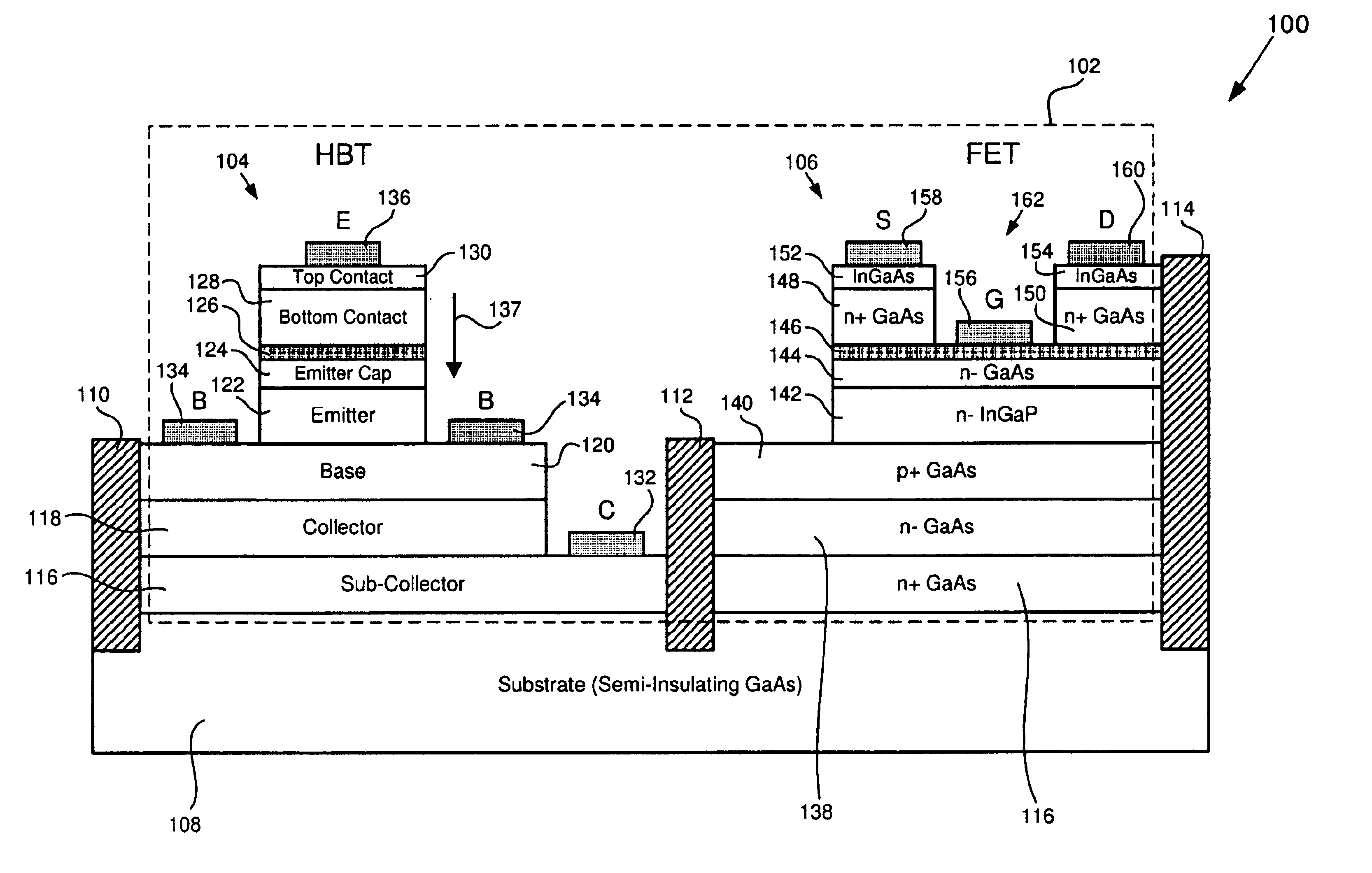
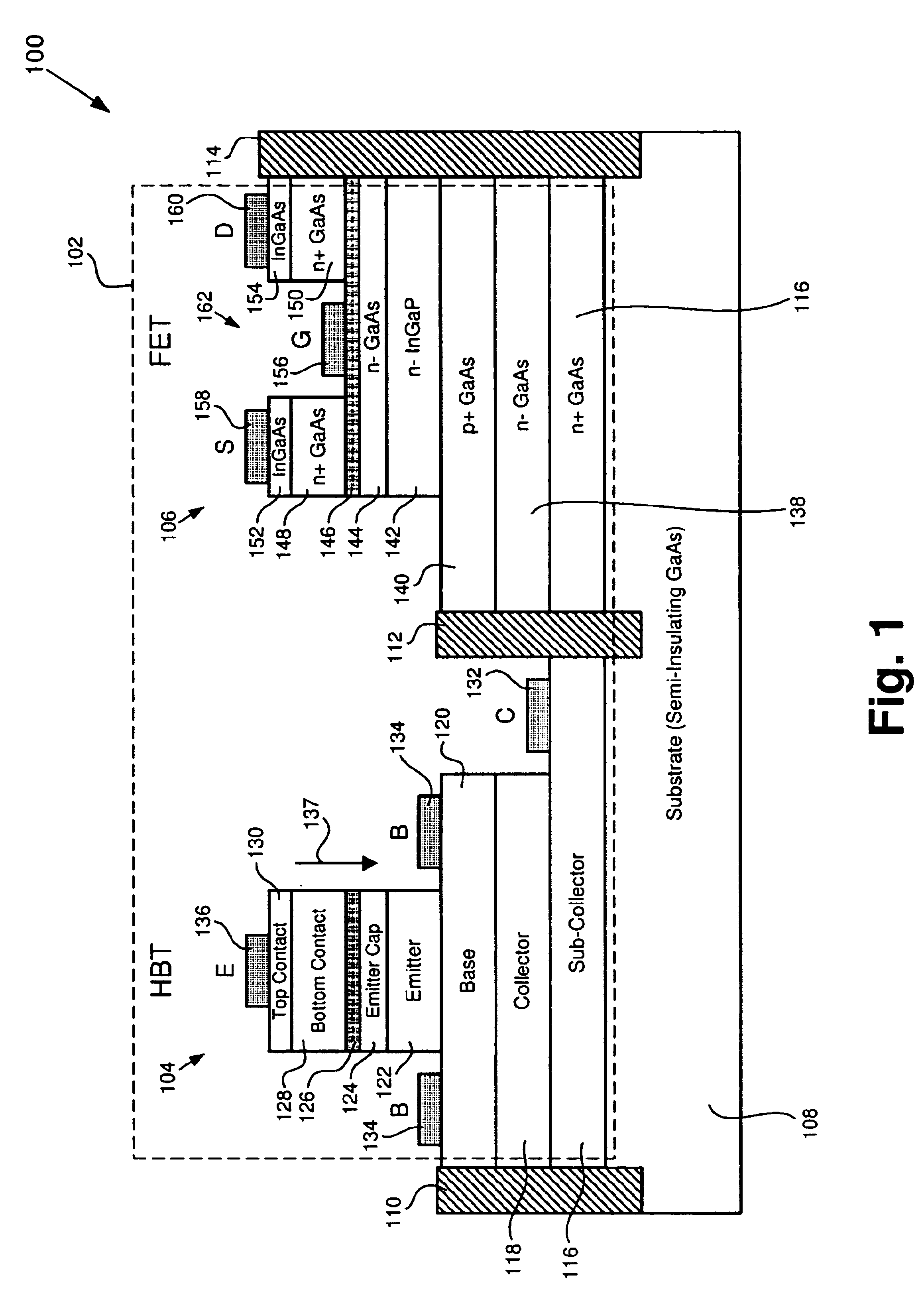
[0013]The present invention is directed to BiFET including a FET having increased linearity and manufacturability. The following description contains specific information pertaining to the implementation of the present invention. One skilled in the art will recognize that the present invention may be implemented in a manner different from that specifically discussed in the present application. Moreover, some of the specific details of the invention are not discussed in order not to obscure the invention.

[0014]The drawings in the present application and their accompanying detailed description are directed to merely exemplary embodiments of the invention. To maintain brevity, other embodiments of the present invention are not specifically described in the present application and are not specifically illustrated by the present drawings. Certain details and features have been left out of FIG. 1, which are apparent to a person of ordinary skill in the art. Although structure 100 illustra...


PUM


Abstract

According to one exemplary embodiment, a BiFET situated on a substrate comprises an emitter layer segment situated over the substrate, where the emitter layer segment comprises a semiconductor of a first type. The HBT further comprises a first segment of an etch stop layer, where the first segment of the etch stop layer comprises InGaP. The BiFET further comprises a FET situated over the substrate, where the FET comprises source and drain regions, where a second segment of the etch stop layer is situated under the source and drain regions, and where the second segment of the etch stop layer comprises InGaP. The FET further comprises a semiconductor layer of a second type situated under the second segment of the etch stop layer. The etch stop layer increases linearity of the FET and does not degrade electron current flow in the HBT.

Description

BACKGROUND OF THE INVENTION[0001]1. Field of the Invention[0002]The present invention is generally in the field of fabrication of semiconductor devices. More specifically, the invention is in the field of fabrication of transistors.[0003]2. Related Art[0004]By utilizing BiFET technology, bipolar transistors, such as heterojunction bipolar transistors (“HBTs”), and field effect transistors (“FETs”) can be integrated on the same semiconductor die to provide devices, such as RF power amplifiers, having increased design flexibility. As a result, a BiFET power amplifier including an HBT and a FET can be advantageously designed to operate at a lower reference voltage than a bipolar transistor power amplifier. Of particular interest to device manufacturers are high power BiFET amplifiers, which can be formed by integrating a FET into a gallium arsenide (“GaAs”) HBT process. However, previous attempts to integrate a FET into a GaAs HBT process have resulted in degraded HBT performance and / o...

Claims


Application Information

Patent Timeline
Patent Type & Authority Patents(United States)
IPC IPC(8): H01L31/0264H01L31/0328H01LH01L27/06H01L29/08H01L29/737H01L29/812
CPCH01L27/0605H01L27/0623H01L29/812H01L29/7371H01L29/0817H01L31/0264H01L31/0328
Inventor ZAMPARDI, PETER J.PIERSON, RICHARD
Owner SKYWORKS SOLUTIONS INC
Why Eureka
Try Eureka