Drive circuit for driving power semiconductor device

a technology of drive circuit and semiconductor device, which is applied in the direction of electronic switching, emergency protective arrangements for limiting excess voltage/current, pulse technique, etc., can solve the problems of reducing the reliability increasing the total cost of the drive circuit, and remarkably delayed short-circuit detection by the collector voltage detector b>6/b>, etc., to achieve higher reliability and reliability. high

Inactive Publication Date: 2005-06-14
NEXGEN CONTROL SYST LLC
View PDF11 Cites 33 Cited by
  • Summary
  • Abstract
  • Description
  • Claims
  • Application Information

AI Technical Summary

Benefits of technology

[0010]The present invention is proposed to solve the above-mentioned problems, and it is therefore an object of the present invention to provide a high-reliability drive circuit for driving a power semiconductor device, capable of promptly detecting occurrence of a short circuit so as to protect the power semiconductor device even when applied to a high-voltage IGBT.
[0011]In accordance with the present invention, there is provided a drive circuit for driving a power semiconductor device, the circuit including a controllable variable value detection unit for detecting an amount of variable controlled by a control unit and applied to the power semiconductor device during a predetermined time period when the control unit receives a turn-on instruction, and an abnormality detection unit for monitoring the controllable variable amount detected by the controllable variable value detection unit so as to detect occurrence of an abnormality in the power semiconductor device. Therefore, the drive circuit can protect the power semiconductor device with higher reliability by promptly detecting occurrence of a short circuit even when the power semiconductor device is resistant to high voltages.
[0012]In accordance with the present invention, there is provided a drive circuit for driving a power semiconductor device, the circuit including an abnormality detection unit for monitoring a controllable variable amount detected by a controllable variable value detection unit so as to detect occurrence of an abnormality in the power semiconductor device, and for validating the detection result of the occurrence of the abnormality only during a predetermined time period after a control unit has received a turn-on instruction. Therefore, the drive circuit can protect the power semiconductor device with higher reliability by promptly detecting occurrence of a short circuit even when the power semiconductor device is resistant to high voltages.

Problems solved by technology

A problem encountered with a prior art drive circuit constructed as above for driving a power semiconductor device is that when the drive circuit is applied to a high-voltage IGBT, a number of high-voltage diodes 5 need to be connected in series and this results in an increase in the total cost of the drive circuit and a reduction in the reliability of the drive circuit.
Another problem is that to distinguish normal turning-on from a short circuit, the above-mentioned transition time period needs to be masked, so short-circuit detection by the collector voltage detector 6 is remarkably delayed and therefore the IGBT 1 cannot be protected.

Method used


Image

  • Drive circuit for driving power semiconductor device
  • Drive circuit for driving power semiconductor device
  • Drive circuit for driving power semiconductor device

Examples


embodiment 1

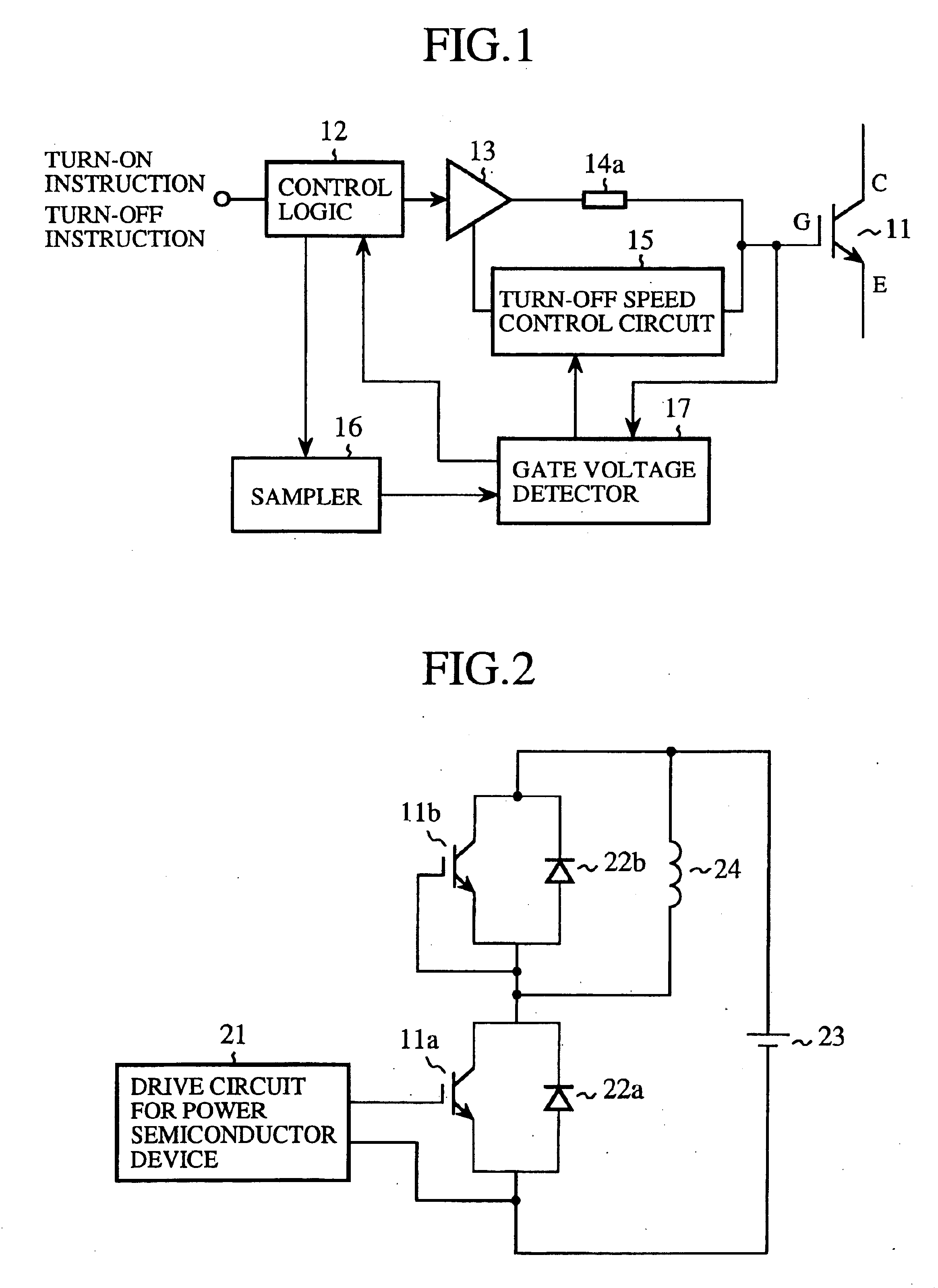
[0039]FIG. 1 is a block diagram showing the structure of a drive circuit for driving a power semiconductor device in accordance with embodiment 1 of the present invention. In the figure, reference numeral 11 denotes an IGBT (Insulated Gate Bipolar Transistor) that is the power semiconductor device driven by the drive circuit. The power semiconductor device is not limited to an IGBT and can be a voltage-driven semiconductor device such as a MOSFET, for example.

[0040]Reference numeral 12 denotes a control logic for sending a gate instruction to turn on the IGBT 11 to a buffer 13 in response to a turn-on instruction from outside the drive circuit, and for sending a gate instruction to turn off the IGBT 11 to the buffer 13 in response to a turn-off instruction from outside the drive circuit. The buffer 13 drives the IGBT 11 according to a gate instruction delivered from the control logic 12. Furthermore, reference numeral 14a denotes an on-state gate resistor, and reference numeral 15 d...

embodiment 2

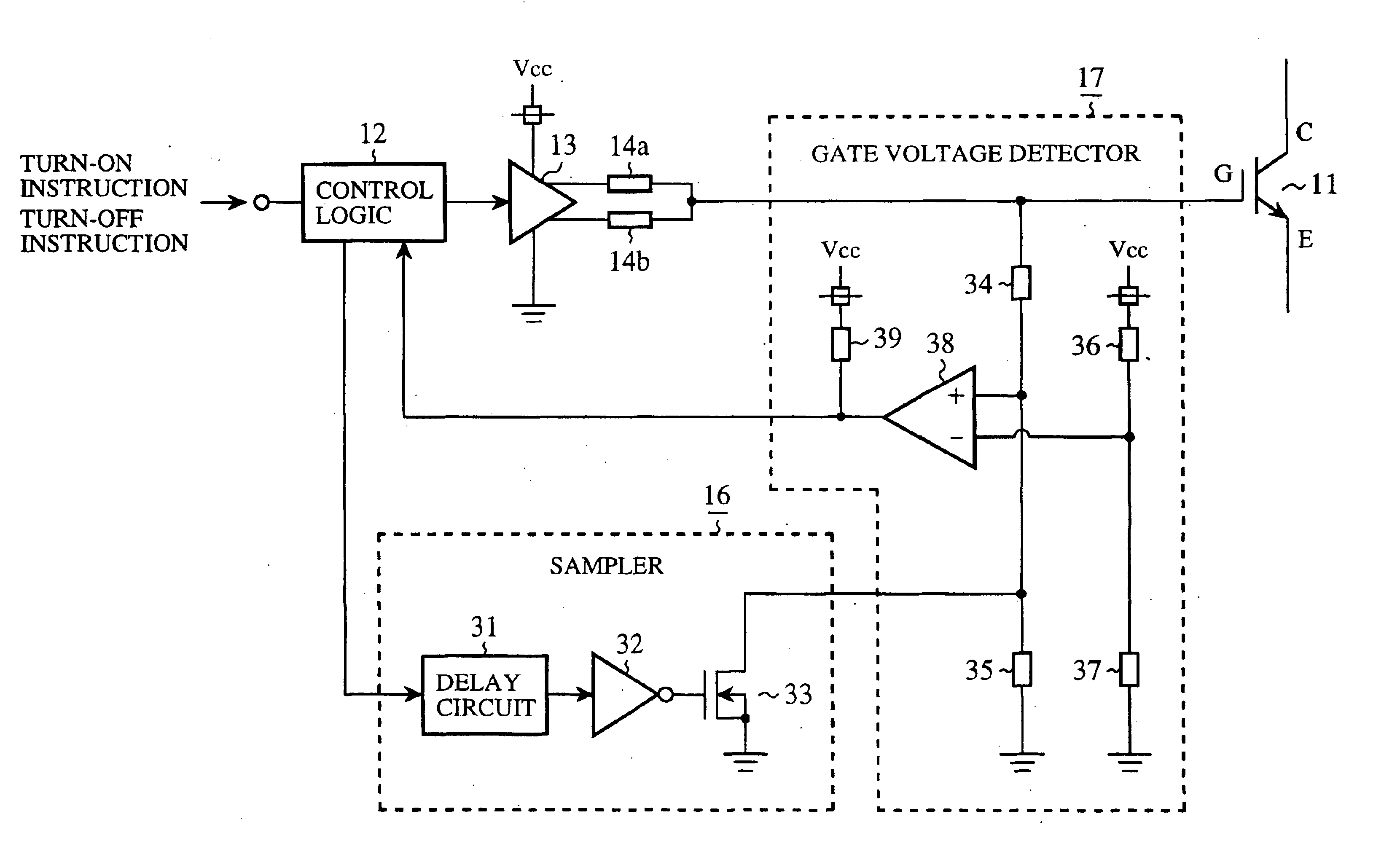
[0060]FIG. 6 is a block diagram showing the structure of a drive circuit for driving a power semiconductor device in accordance with embodiment 2 of the present invention. In the figure, because the same reference numerals as shown in FIG. 1 denote the same components as those of the first embodiment or like components, the explanation of those components will be omitted hereafter. FIG. 6 shows a concrete example of a sampler 16 and a gate voltage detector 17 as shown in FIG. 1. In FIG. 6, a turn-off speed control circuit 15 is omitted, and a buffer 13 connects a gate of an IGBT 11 with a controllable source that sends out a control voltage Vcc when-the IGBT 11 is turned on, and connects the gate of the IGBT 11 with a ground when the IGBT 11 is turned off.

[0061]In FIG. 6, reference numeral 31 denotes a delay circuit that accepts a gate instruction sent thereto from a control logic 12, and sends out the gate instruction after holding it only during a time period from a time t0 to a t...

embodiment 3

[0067]FIG. 8 is a block diagram showing the structure of a drive circuit for driving a power semiconductor device in accordance with embodiment 3 of the present invention. In the figure, because the same reference numerals as shown in FIG. 6 denote the same components as those of the second embodiment or like components, the explanation of those components will be omitted hereafter. Reference numeral 40 denotes a capacitor connected in parallel with a dividing resistor 35.

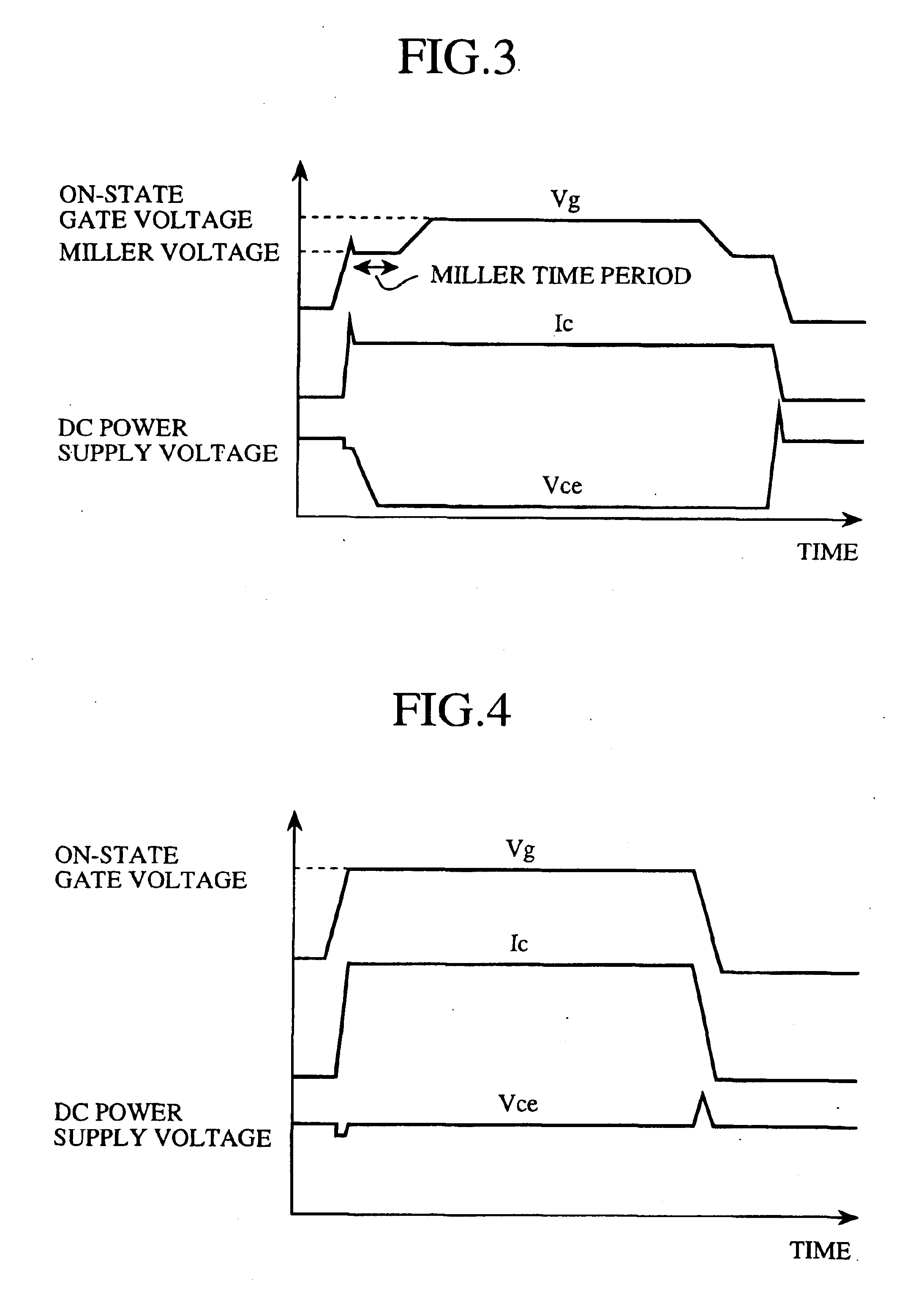
[0068]Hereafter, an operation of the capacitor 40 will be explained. FIG. 9 is an explanatory drawing for showing a gate voltage detection signal (i.e., a divided voltage obtained from a gate voltage Vg by dividing resistors 34 and 35) when no capacitor is connected in parallel with the dividing resistor 35 and when the capacitor 40 is connected in parallel with the dividing resistor 35. Because the gate voltage detection signal has a waveform equal to that of the divided voltage, the waveform is similar to that of...


PUM


Abstract

A drive circuit includes a gate voltage detector that detects a gate-emitter voltage Vge that appears between the gate and emitter of a power semiconductor device throughout a detection time period during which a sampler allows the process of detecting the gate-emitter voltage Vge, and that recognizes the occurrence of an abnormality in the power semiconductor device when the gate-emitter voltage Vge exceeds a reference value. Therefore, the drive circuit can protect the power semiconductor device with higher reliability by promptly detecting the occurrence of a short circuit even when the power semiconductor device is resistant to high voltages.

Description

BACKGROUND OF THE INVENTION[0001]1. Field of the Invention[0002]The present invention relates to a drive circuit for driving a power semiconductor device and for detecting occurrence of an abnormality in the power semiconductor device.[0003]2. Description of Related Art[0004]FIG. 24 is a block diagram showing the structure of a prior art drive circuit for driving a power semiconductor device. In the figure, reference numeral 1 denotes an IGBT (Insulated Gate Bipolar Transistor) that is a power semiconductor device, reference numeral 2 denotes a control logic for sending a gate instruction to cause the IGBT 1 to make a transition to a closed state to a buffer 3 when receiving a turn-on instruction from outside the drive circuit, and for sending a gate instruction to cause the IGBT 1 make a transition to an open state to the buffer 3 when receiving a turn-off instruction from outside the drive circuit, reference numeral 3 denotes the buffer for driving the IGBT 1 according to the gate...

Claims


Application Information

Patent Timeline
Patent Type & Authority Patents(United States)
IPC IPC(8): H03K17/16H03K17/0812H03K17/08H01L21/822H01L27/04H02M1/00H02M1/08
CPCH03K17/168H03K17/08128
Inventor OHI, TAKESHINAKAYAMA, YASUSHITANAKA, TAKESHI
Owner NEXGEN CONTROL SYST LLC
Why Eureka
Try Eureka