Semiconductor optical device and semiconductor laser module using the semiconductor optical device

Active Publication Date: 2005-06-14
MITSUBISHI ELECTRIC CORP
View PDF2 Cites 2 Cited by
  • Summary
  • Abstract
  • Description
  • Claims
  • Application Information

AI Technical Summary

Benefits of technology

[0016]An object of the present invention is to provide a semiconductor optical device which can enhance a degree of freedom in a design of a nonreflective film even

Problems solved by technology

More specifically, it is difficult to make the low-reflectance wavelength range equal to or wider than 100 nm.
In this design procedure, however, the degree of freedom in a design of a nonreflective film of a semiconductor optical device cannot be enhanced because only two kinds of films form the nonreflective film.
With this design procedure, for example, it is impossible to provide a film for efficient heat radiation by a semiconductor laser as a third film in addition to the two films respectively bringing the real part and imaginary part of the amplitude reflectance to zero.

Method used


Image

  • Semiconductor optical device and semiconductor laser module using the semiconductor optical device
  • Semiconductor optical device and semiconductor laser module using the semiconductor optical device
  • Semiconductor optical device and semiconductor laser module using the semiconductor optical device

Examples


first embodiment

[0053

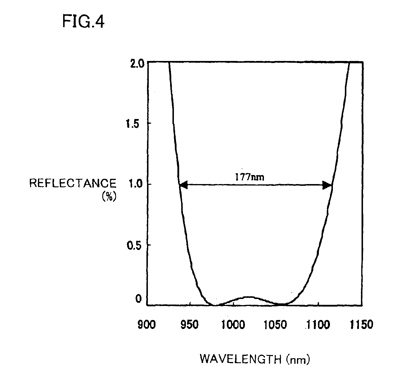
[0054]A description of “a nonreflective film having a two-layer structure which becomes nonreflective at a specific wavelength λ”, which is a base of a semiconductor optical device of this embodiment, will now be given.

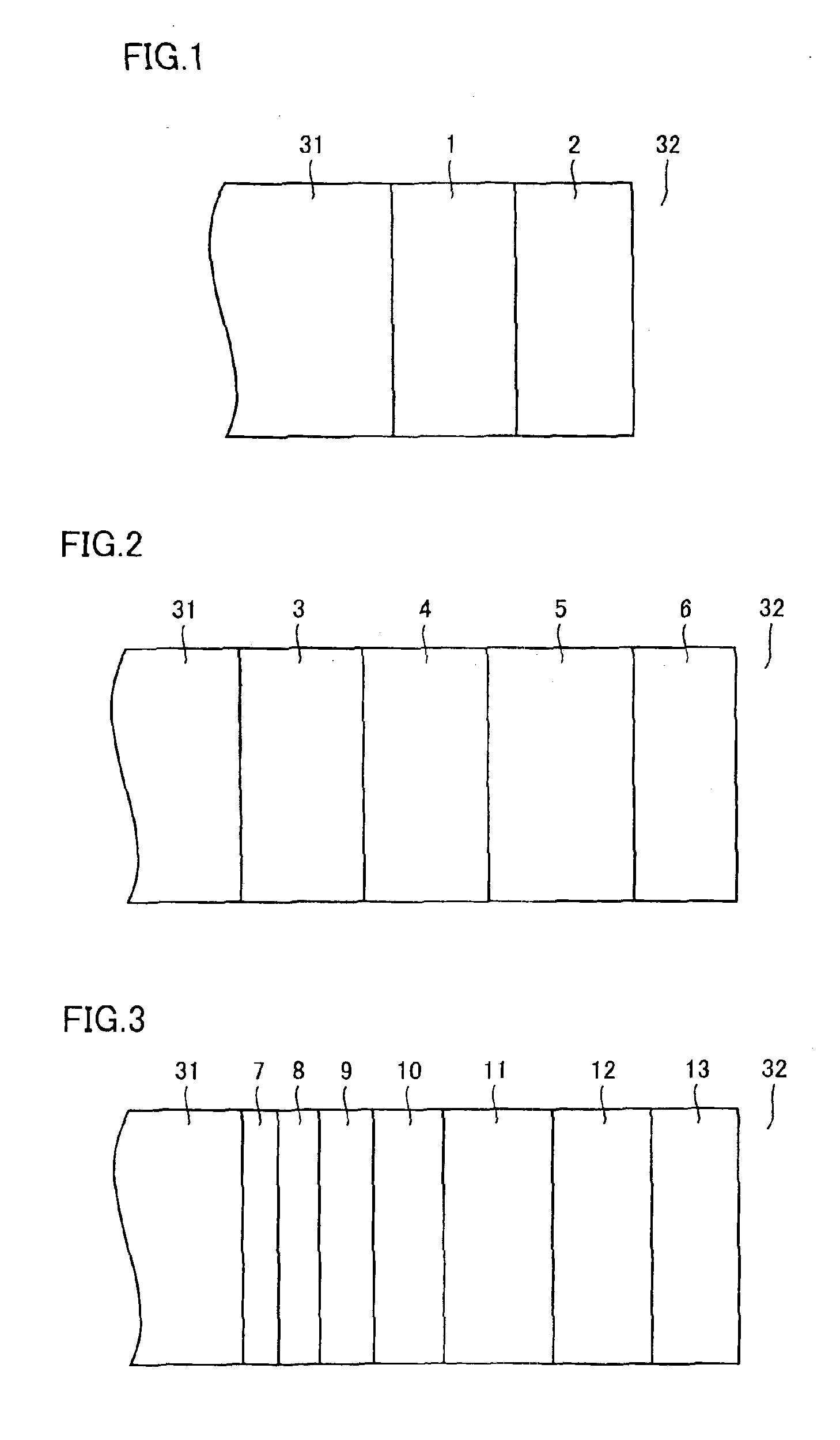
[0055]In a nonreflective film having a two-layer structure shown in FIG. 1, a two-layer structure film formed with a first film 1 having a refractive index n1 and a thickness d1 and a second film 2 having a refractive index n2 and a thickness d2, and a semiconductor laser 31 having an effective refractive index nc are provided in space 32 of air, nitrogen or the like which has a refractive index of 1.

[0056]Assuming that a wavelength of light is λ and unknown phases of first film 1 and second film 2 are φ1 and φ2, respectively, the following equations (1a), (1b) are formulated. ϕ1=2⁢πλ⁢n1⁢d1(1⁢a)ϕ2=2⁢πλ⁢n2⁢d2(1⁢b)

[0057]Herein, an amplitude reflectance r is expressed as the following equation (2). r=(nc-1)⁢cos⁢ ⁢ϕ1⁢cos⁢ ⁢ϕ2+(n1n2-n2⁢ncn1)⁢sin⁢ ⁢ϕ1⁢sin⁢ ⁢ϕ2-i⁢{(ncn2...

second embodiment

[0084

[0085]A semiconductor optical device of a second embodiment will now be described with reference to FIGS. 6-8.

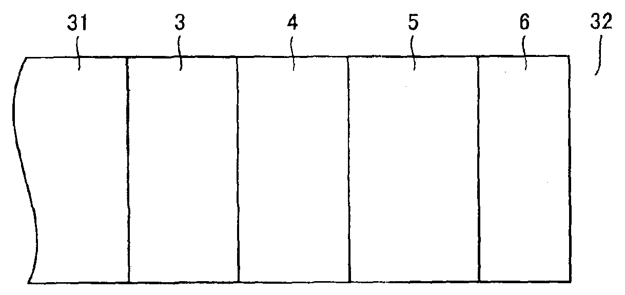
[0086]The semiconductor optical device of this embodiment is formed such that, semiconductor laser 31 and a nonreflective film formed by adding a specific kind of film having known refractive index and thickness to a six-layer structure formed by tripling specific two kinds of films having known refractive indices and unknown thicknesses are provided in space 32 of air, nitrogen or the like which has a refractive index of 1.

[0087]In addition, as shown in FIG. 6, the nonreflective film includes a first film 14 of tantalum oxide (Ta2O5) (refractive index n1=2.057, thickness=Ad1), a second film 15 of alumina (Al2O3) (refractive index n2=1.62, thickness=Ad2), a third film 16 of tantalum oxide (Ta2O5) (refractive index n1=2.057, thickness=Bd1), a fourth film 17 of alumina (Al2O3) (refractive index n2=1.62, thickness=Bd2), a fifth film 18 of tantalum oxide (Ta2O5) (refractive...

third embodiment

[0094

[0095]A semiconductor optical device of a third embodiment will now be described with reference to FIGS. 9-14.

[0096]As shown in FIG. 9, the semiconductor optical device of this embodiment is formed such that, semiconductor laser 31 and a nonreflective film formed by adding a specific kind of film having known refractive index and thickness to a six-layer structure formed by tripling specific two kinds of films having known refractive indices and unknown thicknesses are provided in space 32 of air, nitrogen or the like which has a refractive index of 1.

[0097]In addition, the nonreflective film includes a first film 21 of aluminum nitride (AlN) (refractive index n3=2.072, thickness d3=50 nm), a second film 22 of tantalum oxide (Ta2O5) (refractive index n1=2.057, thickness=Ad1), a third film 23 of alumina (Al2O3) (refractive index n2=1.62, thickness=Ad2), a fourth film 24 of tantalum oxide (Ta2O5) (refractive index n1=2.057, thickness=Bd1), a fifth film 25 of alumina (Al2O3) (refr...


PUM

PropertyMeasurementUnit
Massaaaaaaaaaa
Nanoscale particle sizeaaaaaaaaaa
Reflectanceaaaaaaaaaa

Abstract

A nonreflective film includes films having refractive indices higher than 1 and a high-refractive index film (first film, third film, fifth film) and a low-refractive index film (second film, fourth film, sixth film, seventh film) respectively having refractive indices higher and lower than the square root of an effective refractive index of a semiconductor laser. The films have least three different compositions. Each film has a single composition. The films bring a real part and an imaginary part of an amplitude reflectance to zero, as a whole. Therefore, a semiconductor optical device with an improved degree of freedom in design of the nonreflective film is provided, even when a total thickness of the films is different from one quarter wavelength of the incident light.

Description

[0001]This disclosure is a continuation-in-part of U.S. patent application Ser. No. 10 / 314,966 filed Dec. 10, 2002, now abandoned.BACKGROUND OF THE INVENTION[0002]1. Field of the Invention[0003]The present invention relates to a semiconductor optical device including a semiconductor optical element which emits light, and to a semiconductor laser module using the semiconductor optical device.[0004]2. Description of the Background Art[0005]A structure of a conventional semiconductor optical device, which is disclosed in Japanese Patent Laying-Open No. 2001-196685, will now be described with reference to FIG. 19. As shown in FIG. 19, the conventional semiconductor optical device includes a semiconductor laser 101, which is an example of the semiconductor optical element and which has an effective refractive index nc, and a nonreflective film provided in contact with a light emission surface of semiconductor laser 101.[0006]In addition, the nonreflective film includes a first film 102 p...

Claims


Application Information

Patent Timeline
IPC IPC(8): G02B1/11G02B1/10H01S5/00H01S5/028H01S5/50H01L33/00H01L33/44
CPCG02B1/115H01S5/028H01S5/50H01L33/44
Inventor SHIGIHARA, KIMIOKAWASAKI, KAZUSHIGEMATSUOKA, HIROMASU
Owner MITSUBISHI ELECTRIC CORP
Why Eureka
Try Eureka