Support structures for wirebond regions of contact pads over low modulus materials

a technology of low-modulus materials and support structures, which is applied in the direction of semiconductor devices, semiconductor/solid-state device details, electrical apparatus, etc., can solve the problems of less structural stability of metallization embedded in low-k dielectric materials, low modulus of low-k dielectric materials, and difficulty in wirebonding contact pads having low-k dielectric materials disposed beneath the pads, so as to reduce the chance of damage to the die and increase yield

Inactive Publication Date: 2005-06-21
INFINEON TECH AG +1
View PDF31 Cites 56 Cited by
  • Summary
  • Abstract
  • Description
  • Claims
  • Application Information

AI Technical Summary

Benefits of technology

[0011]Advantages of the invention include providing a structural support within low-modulus material layers beneath the wirebond region of contact pads, decreasing the chance of damaging the die during the wirebonding process and increasing yields. The support structures may be coupled to integrated circuits of the semiconductor device and may function as signal lines or power distribution busses. Interconnect lines for the integrated circuits also may be run between adjacent support structures within each low modulus dielectric layer. Support vias coupled between support structures in adjacent low modulus dielectric layers may be positioned directly over one another, forming a via support stack for exceptional mechanical support under the contact pads.

Problems solved by technology

However, low-K dielectric materials typically have a low modulus and are structurally weak compared to silicon dioxide.
Low modulus dielectric materials strain and deform easily, thus providing less structural stability for metallization embedded in the low-k dielectric.
Wirebonding contact pads having low-K dielectric materials disposed beneath the pads is problematic.
This mechanical stress from the wirebond welding process can damage the contact pads and underlying structures, and cause the contact pads to lift or tear from the silicon substrate, destroying the semiconductor device and decreasing yields.
Because low-K materials have a low modulus and are structurally weak, the die is more susceptible to welding damage, resulting in high levels of mechanical failure due to lifts and tears of the contact pads.

Method used


Image

  • Support structures for wirebond regions of contact pads over low modulus materials
  • Support structures for wirebond regions of contact pads over low modulus materials
  • Support structures for wirebond regions of contact pads over low modulus materials

Examples


Embodiment Construction

[0021]Preferred embodiments of the present invention will be discussed, followed by a discussion of the advantages thereof.

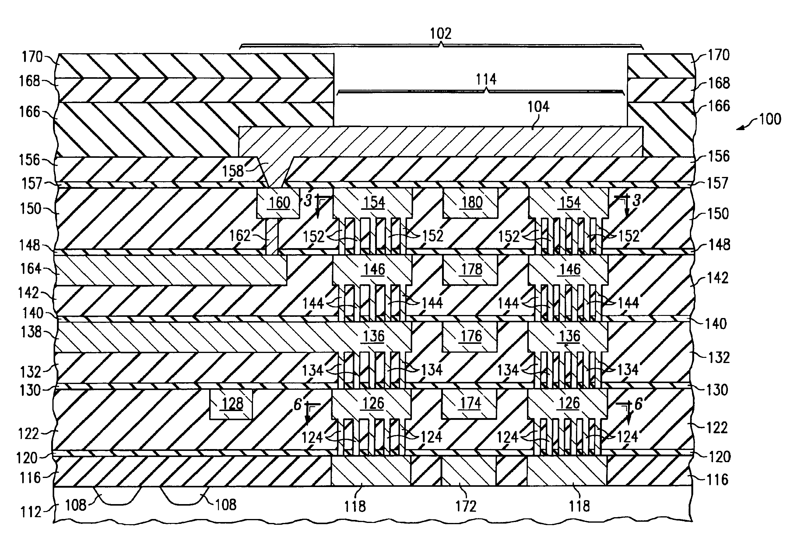
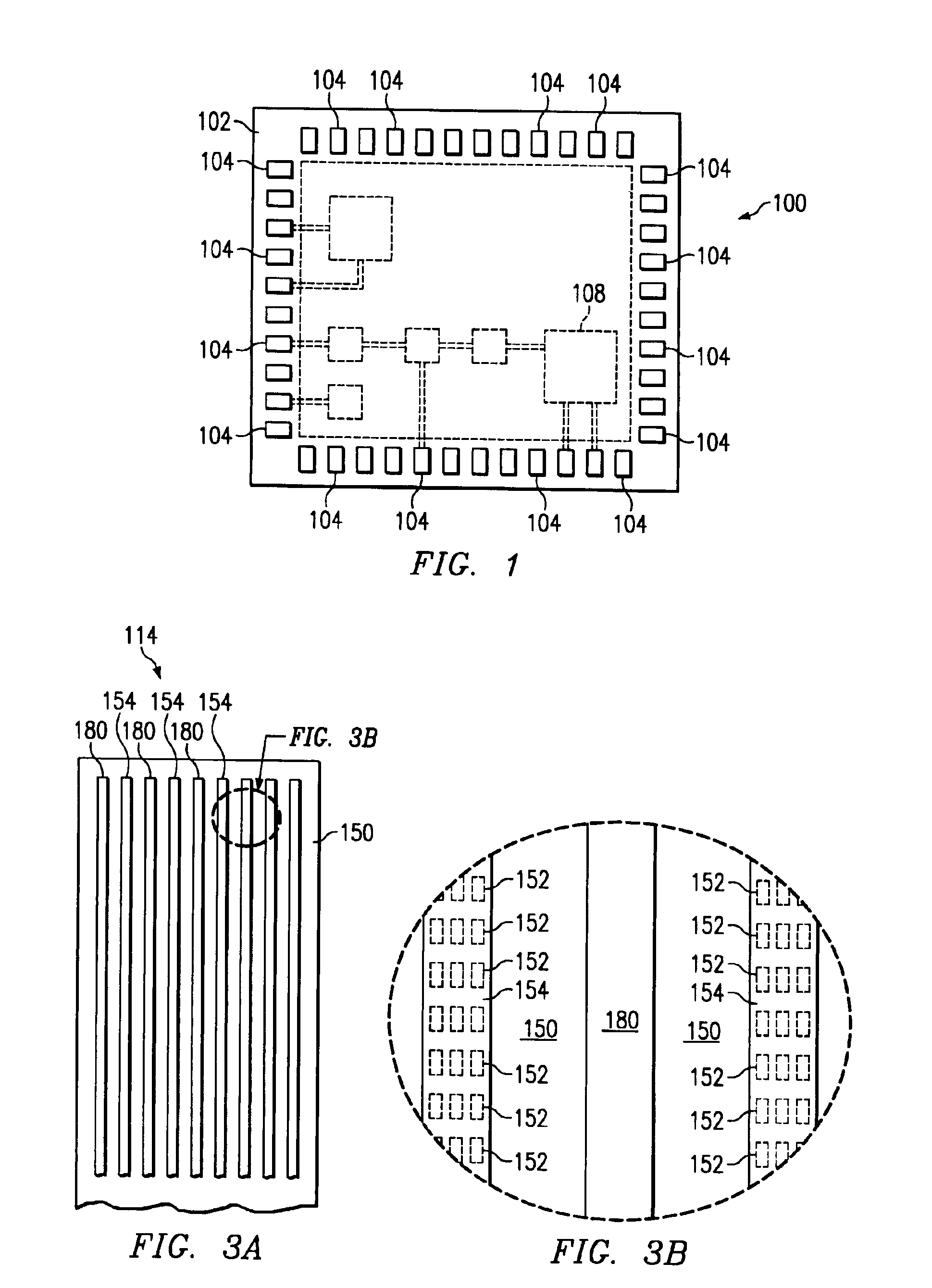
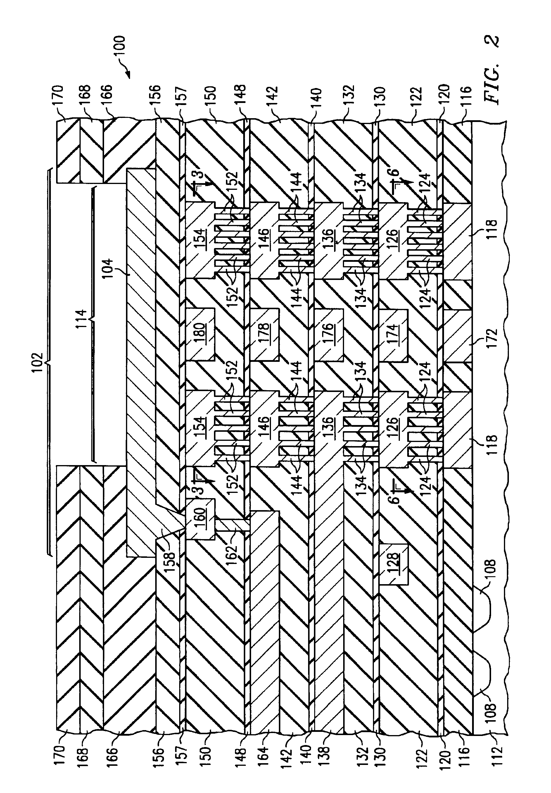
[0022]FIG. 1 illustrates a top view of a semiconductor device 100 in accordance with embodiments of the present invention that comprises at least one contact pad region 102. The contact pad region 102 contains a plurality of contact pads 104 located at the top surface of the semiconductor device 100. The contact pad region 102 may be located at the perimeter or edge of the semiconductor device 100, as shown; however, alternatively, the contact pad region 102 may comprise other areas of the semiconductor device 100, such as the central region, as an example. The device 100 includes one or more integrated circuits 108 formed therein, in underlying layers, for example.

[0023]In accordance with embodiments of the invention, two or more layers of support structures are formed within the low modulus, low-K material layers of the semiconductor device beneath at least th...


PUM


Abstract

A semiconductor device (200) having support structures (218, 226, 236) beneath wirebond regions (214) of contact pads (204) and a method of forming same. Low modulus dielectric layers (216, 222, 232) are disposed over a workpiece (212). Support structures (218, 226, 236) are formed in the low modulus dielectric layers (216, 222, 232), and support vias (224, 234) are formed between the support structures (218, 226, 236). A high modulus dielectric film (220, 230) is disposed between each low modulus dielectric layer (216, 222, 232), and a high modulus dielectric layer (256) is disposed over the top low modulus dielectric layer (232). Contact pads (204) are formed in the high modulus dielectric layer (256). Each support via (234) within the low modulus dielectric layer (232) resides directly above a support via (224) in the underlying low modulus dielectric layer (222), to form a plurality of via support stacks within the low modulus dielectric layers (216, 222, 232).

Description

TECHNICAL FIELD[0001]The present invention relates generally to semiconductor devices, and more particularly to a structure and method of providing mechanical support for contact pads of integrated circuits.BACKGROUND OF THE INVENTION[0002]Semiconductor devices are used in integrated circuits for a wide variety of electronics applications, such as televisions, radios and cellular phones, as examples. There is a trend in the electronics industry towards miniaturization of electronic components, so that electronic devices can be made smaller and lighter. Integrated circuits may comprise multiple levels of metallization for interconnections, and multiple layers of dielectric and semiconductor materials. These layers are patterned using lithography to form conductive lines, transistors, and other elements of integrated circuits.[0003]For a long time, silicon dioxide has been commonly used as a dielectric to isolate conductive lines and various components within the various layers. More ...

Claims


Application Information

Patent Timeline
Patent Type & Authority Patents(United States)
IPC IPC(8): H01L21/60H01L21/02H01L23/485H01L23/48
CPCH01L24/05H01L24/11H01L24/06H01L2224/0401H01L2224/02166H01L2224/04042H01L2224/05546H01L2224/05599H01L2224/05624H01L2224/13099H01L2224/45144H01L2924/01005H01L2924/01006H01L2924/01007H01L2924/01013H01L2924/01014H01L2924/01029H01L2924/01032H01L2924/01061H01L2924/01074H01L2924/01079H01L2924/01082H01L2924/05042H01L2924/10329H01L2924/14H01L2924/30105H01L2924/3025H01L2224/05553H01L2224/48624H01L2924/00014H01L2924/01033H01L2924/01023H01L2924/01019H01L2924/00H01L2224/05093
Inventor BURRELL, LLOYD G.KEMERER, DOUGLASNYE, III, HENRY A.BARTH, HANS-JOACHIMCRABBE, EMMANUEL F.ANDERSON, DAVIDCHAN, JOSEPH
Owner INFINEON TECH AG
Why Eureka
Try Eureka